Understanding analog to digital converters
December 8, 2019 • tutorial • updated February 9, 2020
When working with microcontrollers we sometimes forget that the real world does not just consist of 1's and 0's. It is what we call analog, and in this article we will learn on how to convert analog values from the real world (like the position of a potentiometer) into a digital number consisting of 1's and 0's.
Analog vs. digital

In the real world we are used to an infinite variety of colors, shapes, sounds, volumes, and much more. On a computer, however, everything has to be represented in terms of logical bits and bytes. Computers use the binary system and therefore everything continuous that exists in the real world has to be mapped to something discrete.
Care for an example? Look at the above sunset. If you have ever seen one in real life, you can imagine the perfect gradient from orange to yellow. But on a computer we only have a finite number of colors. We also only have a finite number of pixels. So if you compare the left “analog” situation to the right “digital” situation, you see that it has been pixelized, or, in other words, discretized.
I am quite aware that this example is not very accurate. The picture above already is on a computer (your computer or phone that you are reading this text from). But I hope you get the idea.
Here is a less pretty and poetic, but more tangible example. Imagine you are building a circuit that is supposed to measure a voltage. It should not just measure ON or OFF, but also the magnitude of a signal. This is what an analog to digital converter (or ADC for short) does. It takes a continuous, real world quantity (like a voltage) and converts into a binary number.
Imagine you want to measure how a signal changes over time:
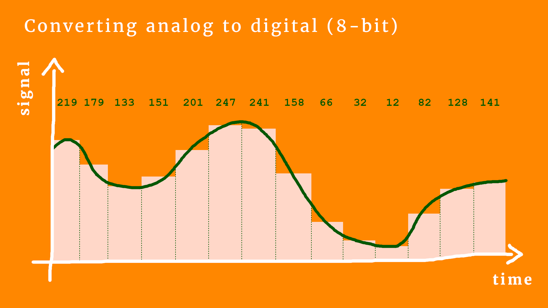
The solid, green line is the continuous signal that can take many values. The ADC converts that quantity into a discrete number (written at the top in the green font). The white bars visualize that number. You see that the numbers have steps and are not continuous, unlike the green line. You also see that the white bars have a duration. This is very characteristic for ADCs:
- The resolution of an analog to digital converter tells you how close it can look. In the above diagram we see an example of 8 bit, meaning that the resulting digital number can be from 0 to 255. Read more about bits and bytes here.
- The reference is the maximum value the signal can take. In the above, the maximum is 255 because the ADC is an 8 bit ADC. If it was a 10 bit ADC, that number would be 1024, and so on. You get it :) In a real world application we typically have to set the reference in form of a voltage. If it is set to, say, 5V, then a signal of 5V will be converted into 255, and a signal of 2.5V will be converted into 127. I hope that makes sense :)
- The conversion time is visualized by the width of the white bars. It takes the ADC some time to convert a signal into a number, and further below we will understand in more detail why this is so. In general the conversion time and the resolution are inversely proportional. If you need a fast result it will be rather inaccurate, but if you need a super accurate result than the conversion time will be slow.
Basic principle of ADCs
Okay, so now that we have some basic idea of what analog to digital converters do, let us understand next how they do it. Here is a simple example sketch:

Okay, there is a lot going on in this schematic. Click here if you want to learn more about reading schematics. Let's go through the main components before we explain how everything works.
- The signal is connected at the jumper called U (because here the signal is a voltage).
- The reference is connected to the jumper REF, and it is also a voltage.
- C is a capacitor, and R is a resistor.
- The switch S, when turned left, charges the capacitor, and when the switch is turned to the right, the capacitor is discharged via the resistor R.
- The integrated circuit IC is a comparator. It has two inputs called + and -. The output of the comparator is 1 when + is larger than -, and 0 when + is less than -. That makes sense, right? It compares the two inputs!
- And the thing on the very right is a timing circuit that I visualized as a simple clock.
So how does it work? We can divide the process into three stages:
- The switch is in the left position, and the capacitor C is charged to the current value of the signal at the U jumper. This is also called acquisition.
- When the switch is turned to the right, the capacitor is discharged. Also, the clock is turned on and starts counting. I won't go into the details here, but when you discharge a capacitor C over a resistor R, the voltage cuts in half roughly every 0.7RC seconds. So the capacitor C is being discharged.
- When the voltage stored in the capacitor reaches the reference voltage, the comparator kicks in. The signal at + is no longer greater than that at -! This means that the output of the comparator turns ON and stops the timer. This process is called conversion. Now that we have the time it took to reduce the signal from U to REF, we can calculate U if we know the values of REF as well as R and C. The formula is written in the diagram above.
And that's it! Granted, I described it a bit schematically, but in principle that is exactly how it works. And now we can also understand the role played by the resolution and conversion time: the better the accuracy of the reference voltage, and the higher the resolution of the timing circuit, the more accurate the reading will be. Also, the larger the capacitor C, the higher the conversion time. But it is also a trade off: if the capacitor is very large, the acquisition time becomes longer, but the accuracy of the timing circuit does not have to be very good either :)
Using the ADC module of a PIC microcontroller
Okay, let's look at a concrete example! You see, many PIC microcontrollers come with a built-in ADC module. Here we will look at the PIC16F1455, which is a neat little 14-pin controller. Today we will use it to read out the position of a potentiometer:
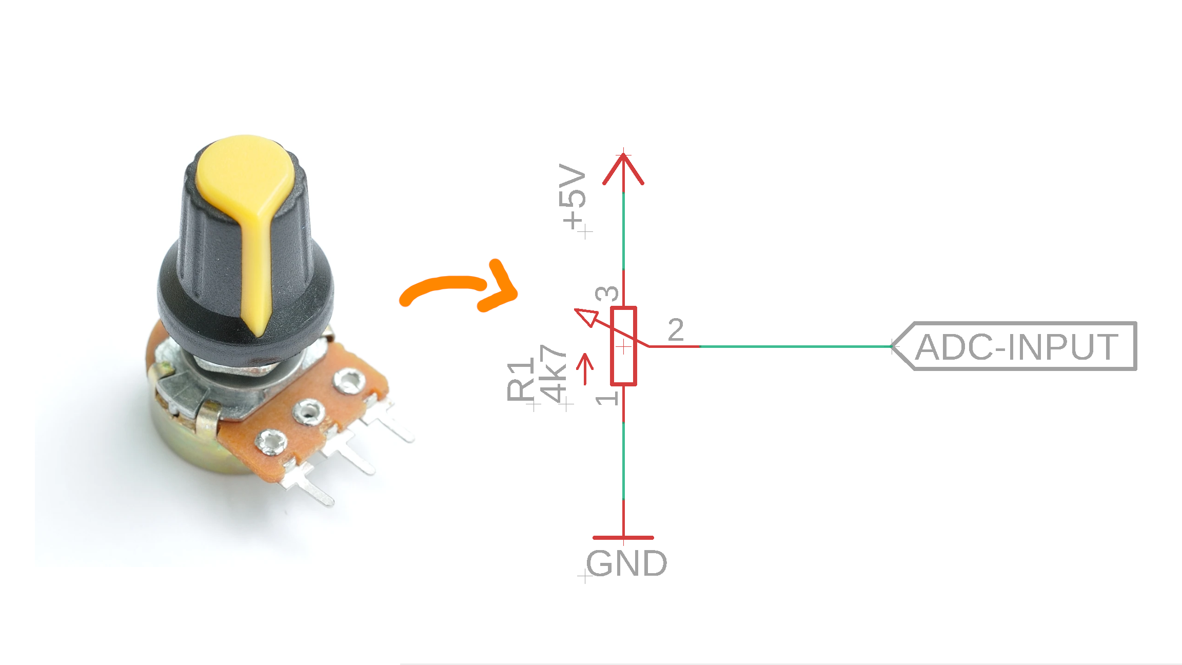
Depending on the position of the yellow marker, this potentiometer will have a value of 0-4.7kΩ, and our goal is to convert that position into a number between 0 and 1023. All we have to do is connect the middle pin to the ADC input of our PIC16F1455. Here you can see the pinout of the PIC16F1455:
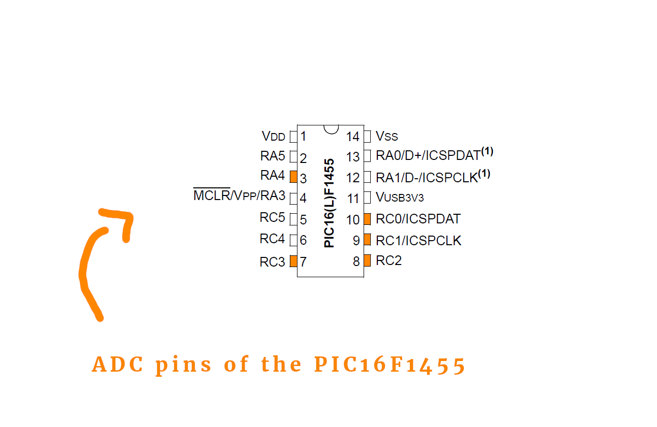
All ADC inputs are highlighted in orange, and, as you can see, there are many of them! The PIC16F1455 only has one built-in ADC module, however, and we have to control with our software (see below) which analog input is connected to the ADC module.
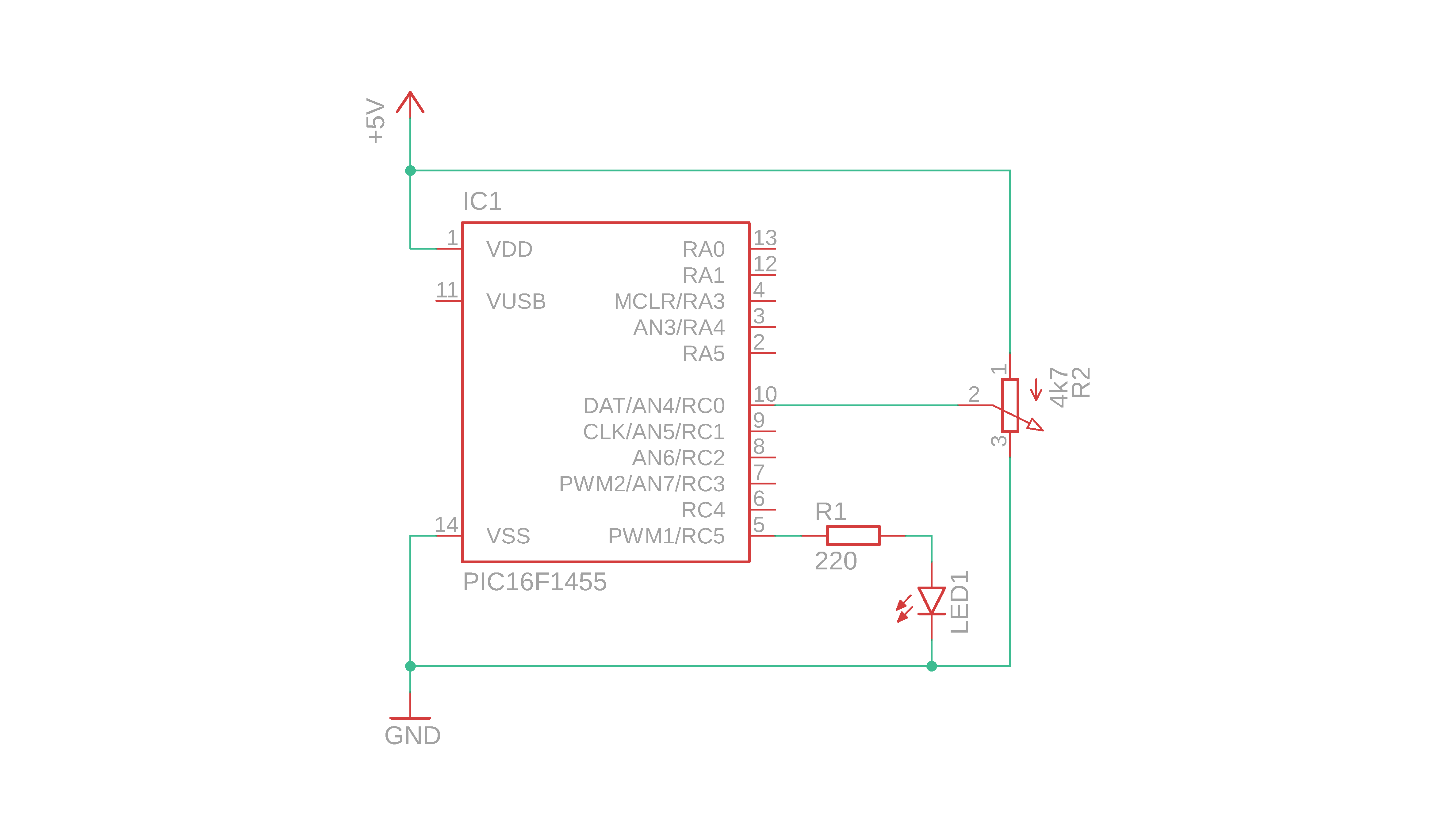
Our little test circuit is very simple: we will convert the position of the potentiometer into a number from 0-1023 (because the PIC16F1455's ADC module has a resolution of 10 bit) and then we will use pulse-width modulation to adjust the brightness of an LED accordingly. The PIC16F1455's PWM module also has a resolution of 10 bit, so we can just take the 10 bit ADC conversion result and write it into the duty-cycle register of the PWM module.
Here is the quite simple schematic:
Now let's take a look at the important bits of the source code (see the full code in the appendix, and download the main.c file as well as the compiled .hex-file in the resources box).
We configure the PIC16F1455 to run on its 4MHz internal oscillator so that we can save external components. Then we initialize the ADC module as follows:
	// ADC settings

	// ADC sampling frequency per bit is F_osc/16
	ADCS0 = 1;
	ADCS1 = 0;
    ADCS2 = 1;

    // result alignment
    ADFM = 0;

	// RC0 as analog input
	TRISC0 = 1;
    ANSC0 = 1;

    // select channel AN4 (which corresponds to RC0)
    CHS0 = 0;
    CHS1 = 0;
    CHS2 = 1;
    CHS3 = 0;
    CHS4 = 0;

	// turn the ADC on
	ADON = 1;
- In lines 45-48 we set the conversion time for the ADC module, and we set it to the lowest possible speed because this circuit does not have to be very fast, so we can instead aim for accuracy. (Strictly speaking we also don't need accuracy since we are just adjusting the brightness of an LED, but I am just writing what we are doing so that you can decide for yourself what you prefer.)
- In line 51 we adjust the alignment. What is that? Well, the PIC16F1455 is an 8-bit microcontroller but its ADC module has a resolution of 10 bit, which means that these ten bits have to be distributed on two registers, see more below. Line 51 corresponds to one possible option, see also the datasheet on page 152.
- Lines 53-55 set the AN4 pin (pin RC0) to the analog input mode. It is very important to set the
ANSC0bit to 1, because otherwise the ADC features are disabled on that pin. - Then, in lines 57-62, we select channel AN4 to be the active analog input channel. If we wanted to read out instead, say, AN1, we would have to change those lines. Check out section 16.3, page 155, in the PIC16F1455 datasheet to learn how.
- Finally, in line 65, we can turn the ADC module on. The reference voltage of the ADC module, if not specified otherwise, is set to +5V automatically (or whatever voltage you run your circuit with). This means that one full revolution of the potentiometer will give the result of 1023.
Then we set up the PWM module, which is similar to what we learned in the PWM article. Here is the relevant code:
	// PWM settings

    // PWM1 module is RC5
    TRISC5 = 0;

    // configure TIMER2
    PR2 = 0xff;
    T2CON = 0b100;

    // turn on PWM module
    PWM1EN = 1;
    PWM1OE = 1;
- Line 70 sets the PWM output pin to be configured as a digital output.
- In lines 72-74 we set the PWM resolution to 10 bit (line 73) and the PWM frequency to around 4kHz (line 74). Learn more about these details in our tutorial on how to adjust the brightness of an LED using pulse-width modulation (PWM).
- Last, in lines 76-78 we turn the PWM module on and enable the corresponding output.
- The PIC16F1455 has a second, independent PWM module, called module 2, which we do not use in this tutorial.
And then comes the main loop:
    // main loop
    while (1) {

		// read 10-bit ADC value
        GO = 1; while (GO);

        // set 10-bit duty cycle value for PWM module
        PWM1DCH = ADRESH;
		PWM1DCL = ADRESL;

        // wait a bit
        __delay_ms(1);

    }
- This main loop gets repeated over and over and over.
- In line 84 the magic happens: we tell the ADC to start a conversion! This is very simple, all we have to do is set the
GObit to 1. After that we wait in a loop until theGObit is zero again, which happens after a successful conversion. - This
while (GO);command is OK for this little example, but it is not recommended for bigger programs: it effectively pauses the entire program until the conversion is completed, and thereby wastes potentially useful computation time and performance. In a better program we should use interrupts, as we already learned in the article on how to create a 1Hz signal with a PIC controller, but I will leave this topic for another time. - Okay, so after that the conversion result is stored in the 8-bit variables
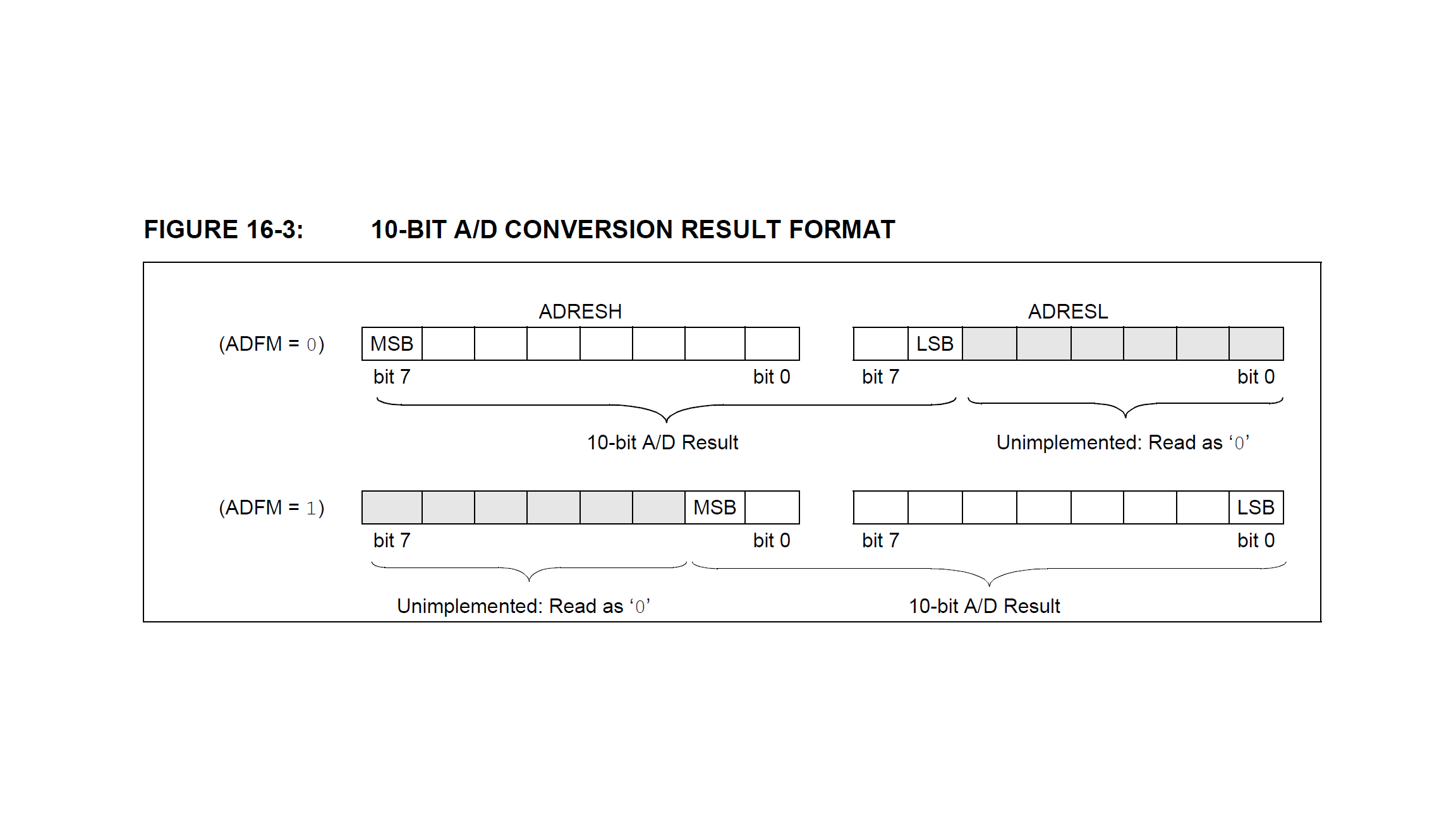
ADRESHandADRESL. We need two of them because the result is a number between 0-1023, which does not fit into one byte (that only goes from 0-255). In lines 71-74 we take those values and insert them into the two duty-cycle registers of the PWM modulePWM1DLHandPWM1DCL(which are, again, two variables, because the 10-bit duty-cycle value does not fit into a single byte). Having setADFMto zero in line 51, the registerADRESHcontains the eight most significant bits andADRESLcontains the two least significant bits. See this diagram here:
- For this choice of
ADFMall we have to do is setPWM1DCH = ADRESHandPWM1DCL = ADRESL. - And then, finally, in line 91 I put a small break of 1 millisecond so that we can save some power and let the controller rest for a bit in this non-time critical application.
And that's it! Wasn't that easy? Sure, dimming an LED with the turn of a button might sound a bit boring, but remember: you understand everything about it! Isn't that great?
Now it is time to compile the source code and flash it onto the PIC16F1455 microcontroller. If this confuses you: no worries :) Have a look at our LED blink tutorial that contains a basic introduction!
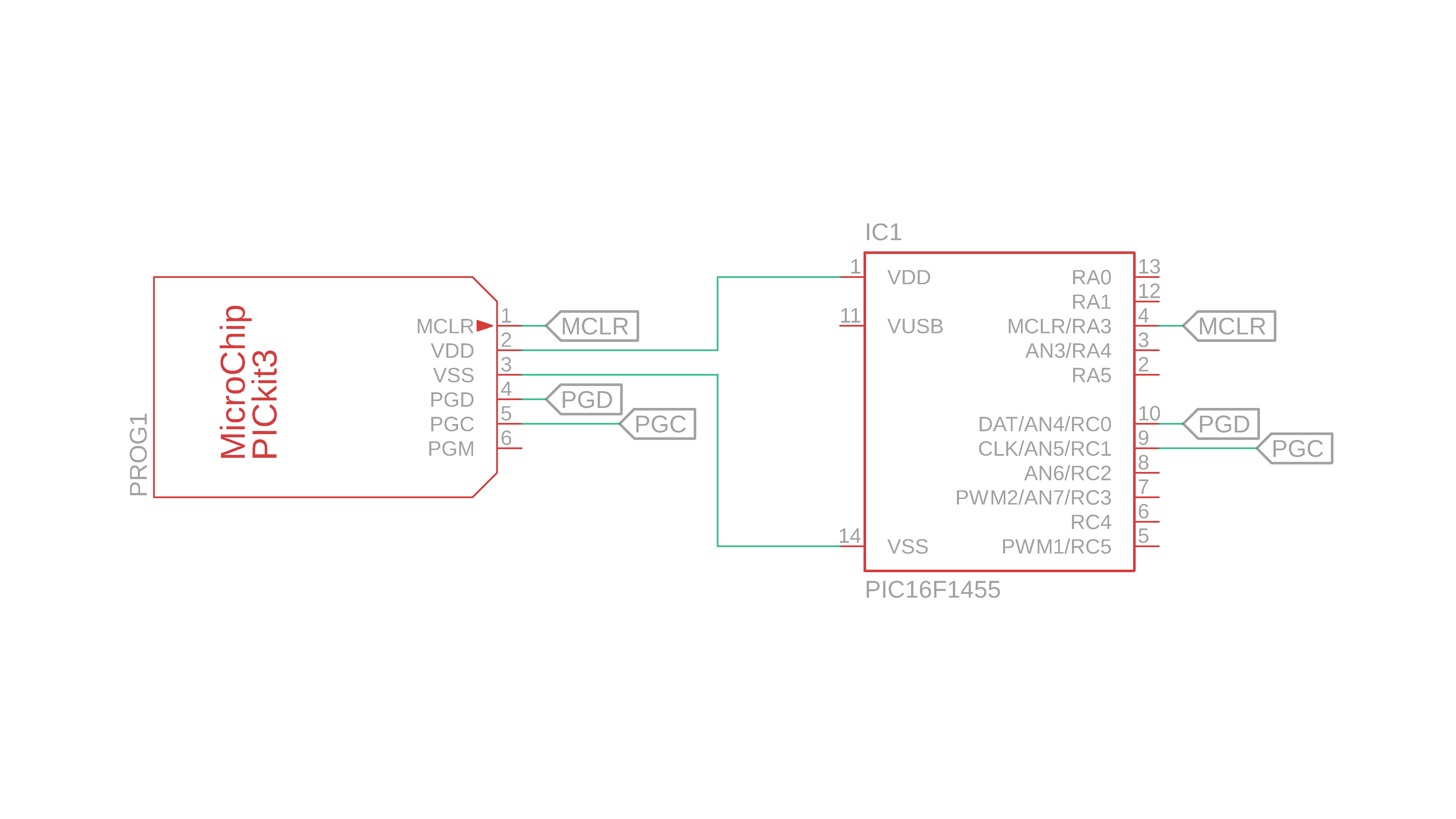
After you have used the freely available MPLAB X IDE and XC8 compiler to turn the above source code into a .hex file, we need to connect the PICkit3 programmer to the PIC16F1455 as follows:
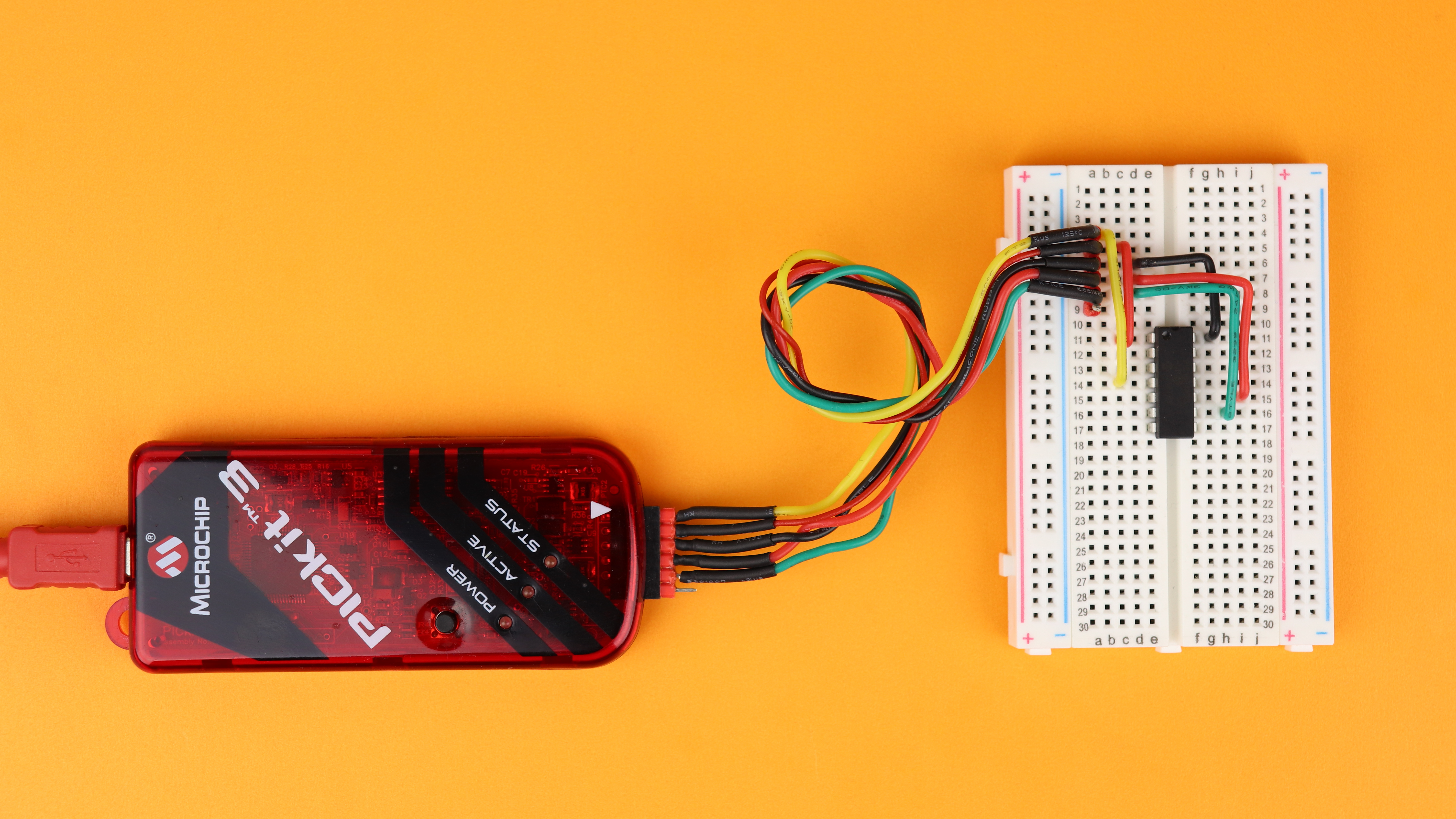
Here is a picture:
Then you can just open the .hex file with MPLAB X IPE, and flash the .hex file onto the PIC161455. After that, the code is stored on the microcontroller and after we connect the microcontroller to power, it will work as we desire :)
Building the test circuit
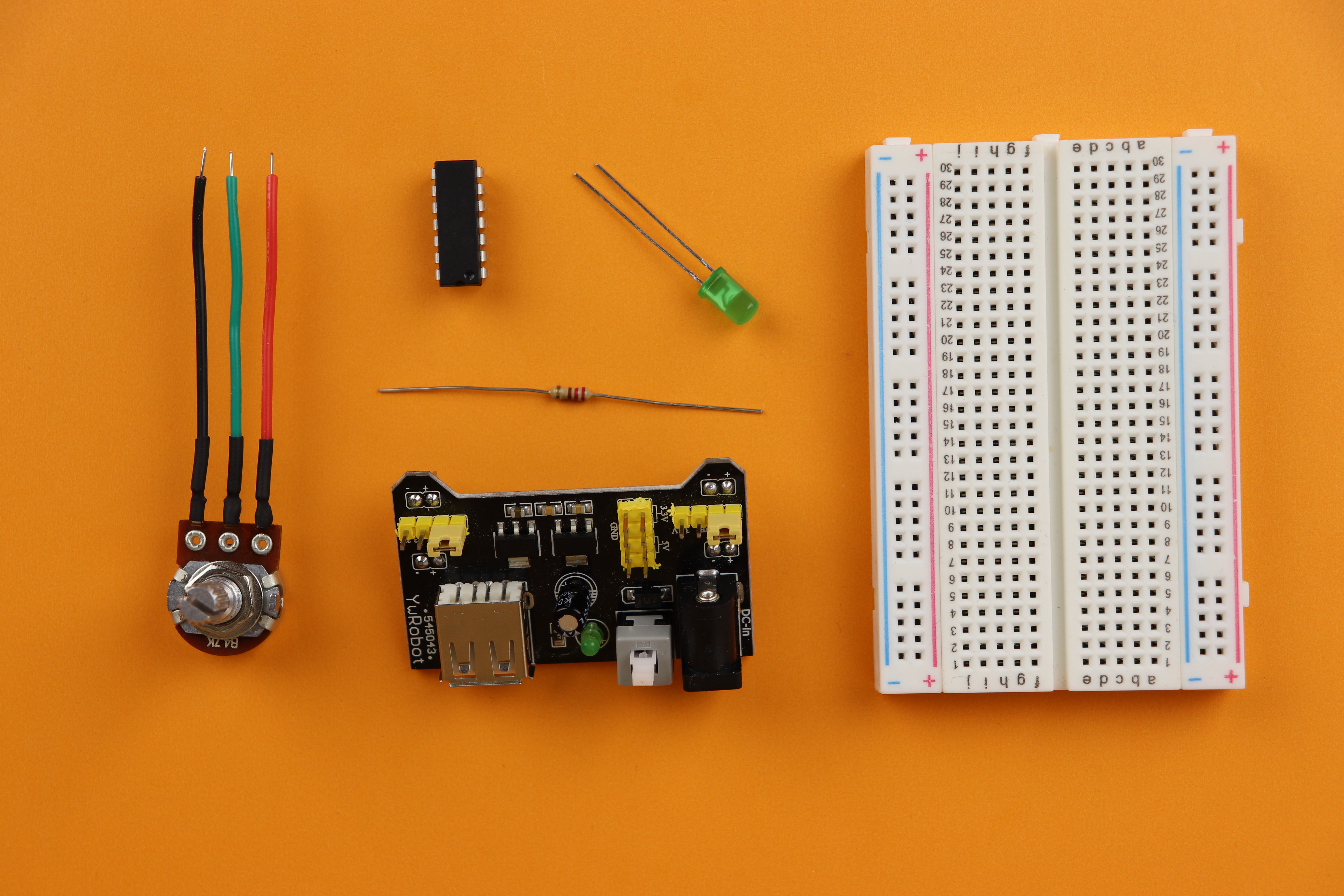
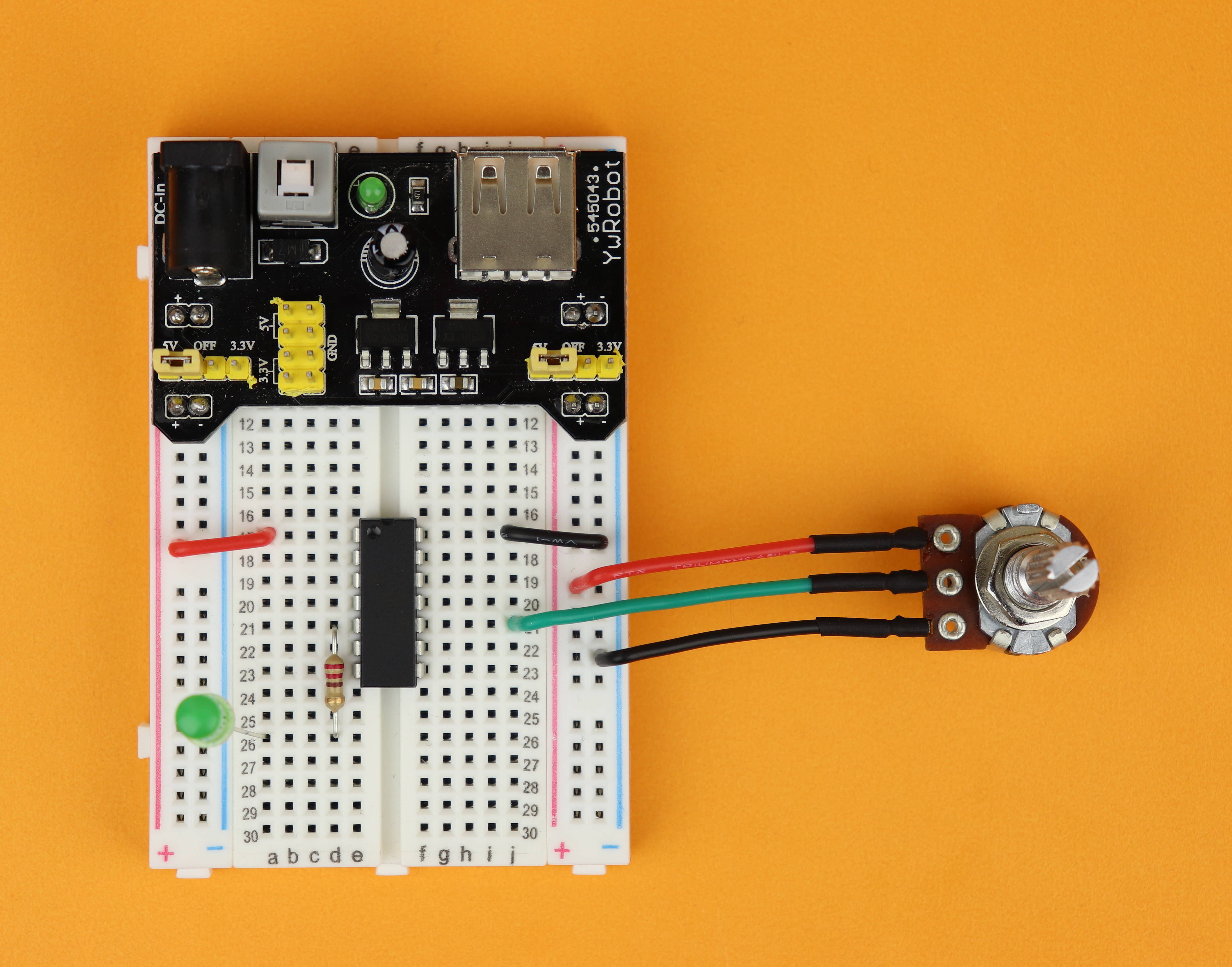
With the microcontroller flashed, we can now build the circuit. Here is an overview of what you need:
And that's all! If you are wondering where to buy the components check out the detailed components box with links and extra information. I chose a 4.7kΩ potentiometer, but 5kΩ, 10kΩ, 22kΩ and even 47kΩ potentiometers should all work fine as well.
Okay, let's get to building! Here is a step-by-step list:
-
-
Step 1
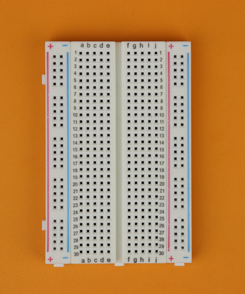
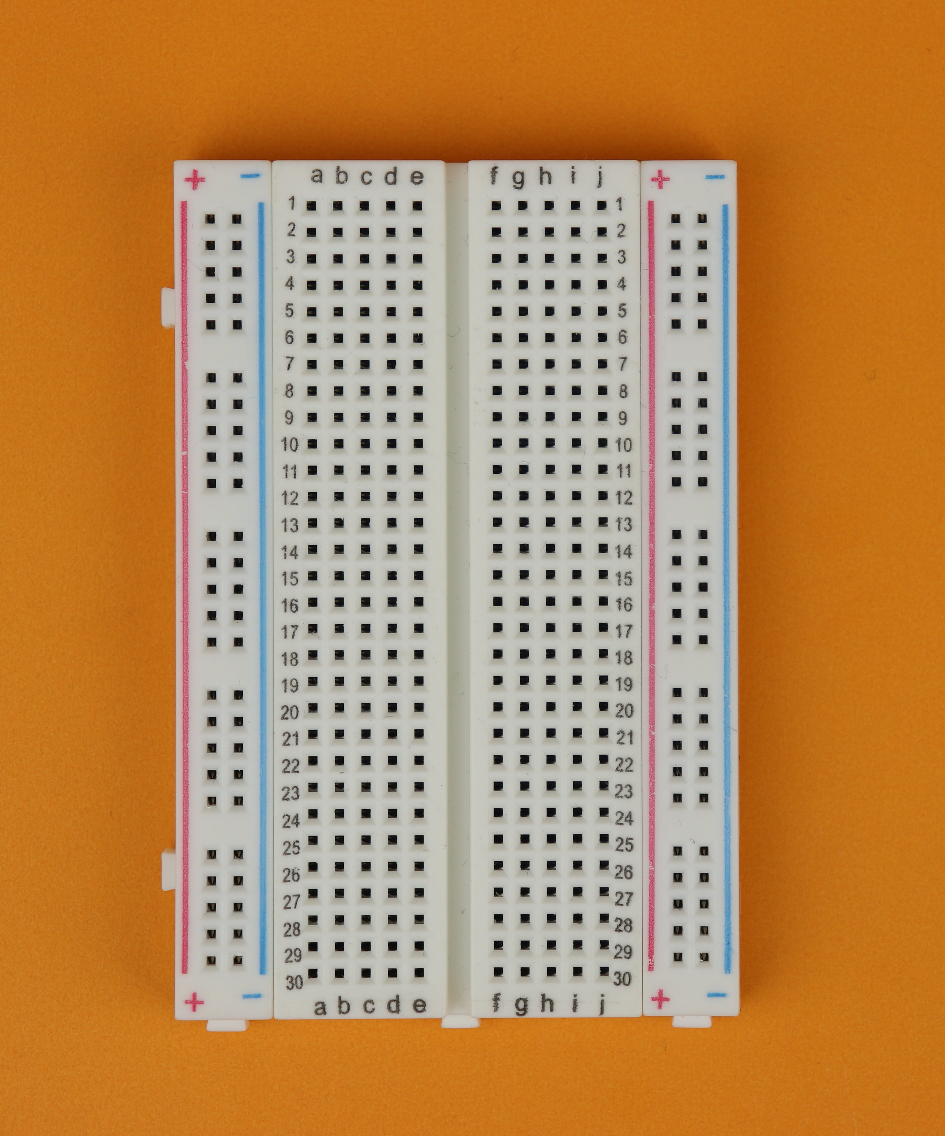
Place the 400-pin breadboard in front of you :) We will call the blue lines the VSS or ground rails, and the red lines the VDD rail. They will later carry the operating voltage for our circuit.
You can read more about breadboards here.
-
-
Step 2
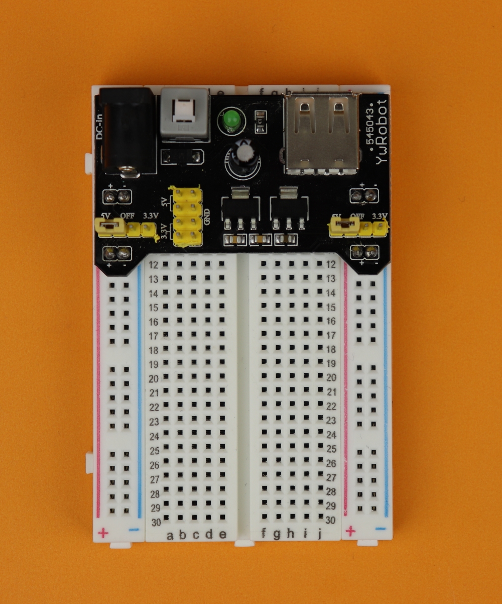
Insert the USB breadboard power supply in the upper part of the breadboard. Make sure the jumpers are set to 5V (and not to 3.3V), because otherwise the LED will not reach its maximum brightness.
-
-
Step 3
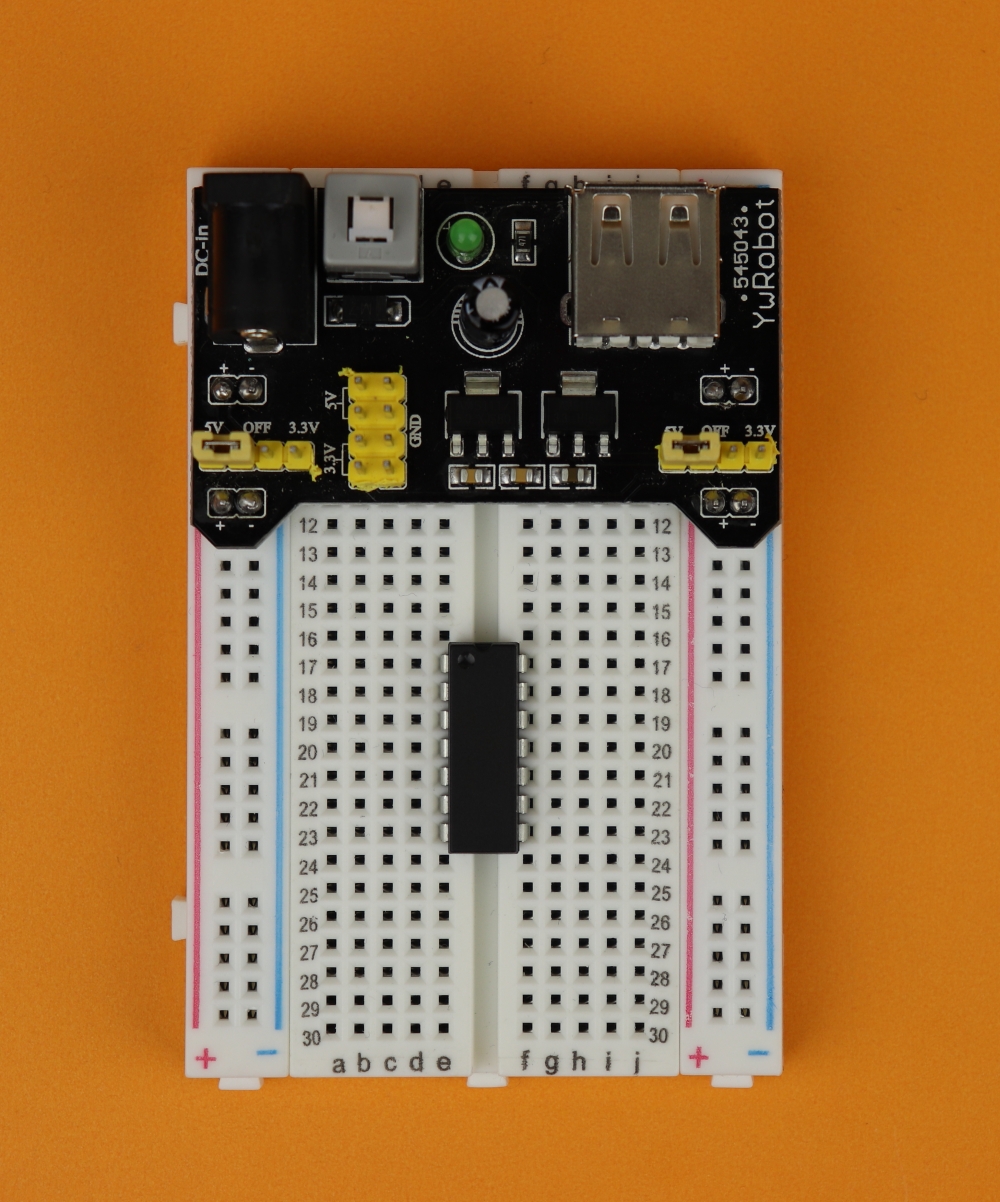
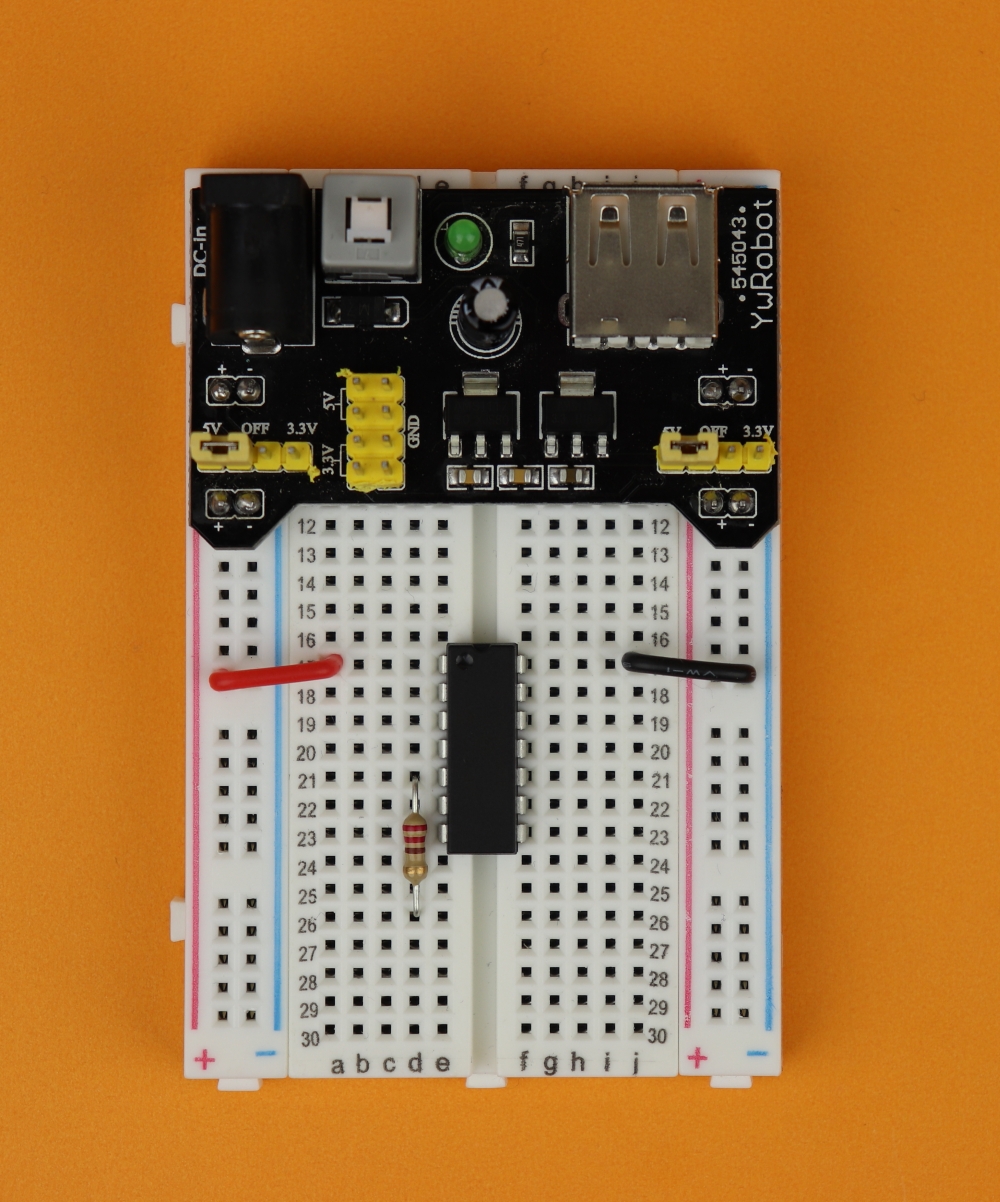
Insert the PIC16F1455 microcontroller in row 17, and make sure the notch points up, as seen in the image.
-
-
Step 4
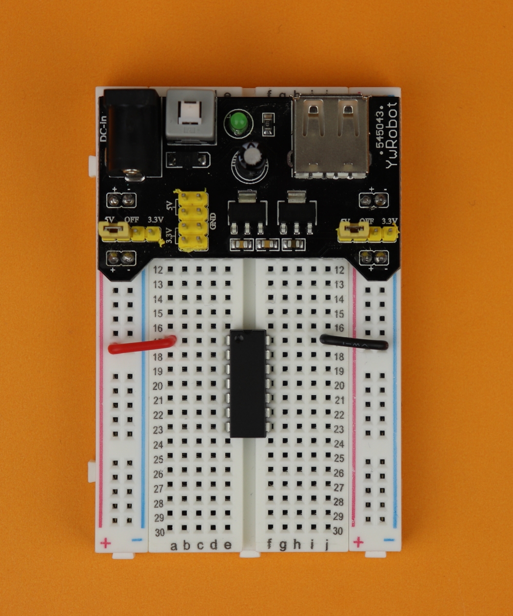
Connect pin 1 of the PIC16F1455 to VDD (the red wire), and pin 14 of the PIC16F1455 to VSS (the black wire).
-
-
Step 5
Insert the 220Ω resistor between pin 5 of the PIC16F1455 (row 21, port RC5) and row 26.
-
-
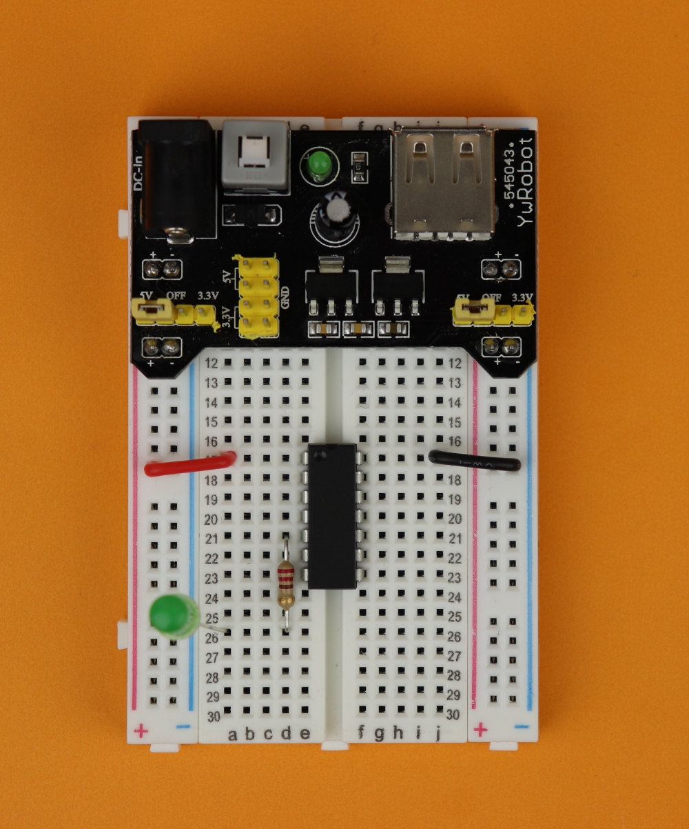
Step 6
Insert the LED: connect its anode to row 26, and its cathode to the ground rail. If you mix up anode and cathode, the LED will not light up.
-

-
Step 7
Insert the potentiometer. Connect its central pin to pin 10 of the PIC16F1455 (row 21, port RC0). Connect the other two terminals to VDD and VSS.
It does not matter which terminal you connect to VDD and which one to VSS. If you switch them, what will happen is that the LED will be turned all the way ON when the potentiometer is turned all the way, say, left, and after switching the connections it will be ON when the potentiometer is turned all the way to the right.


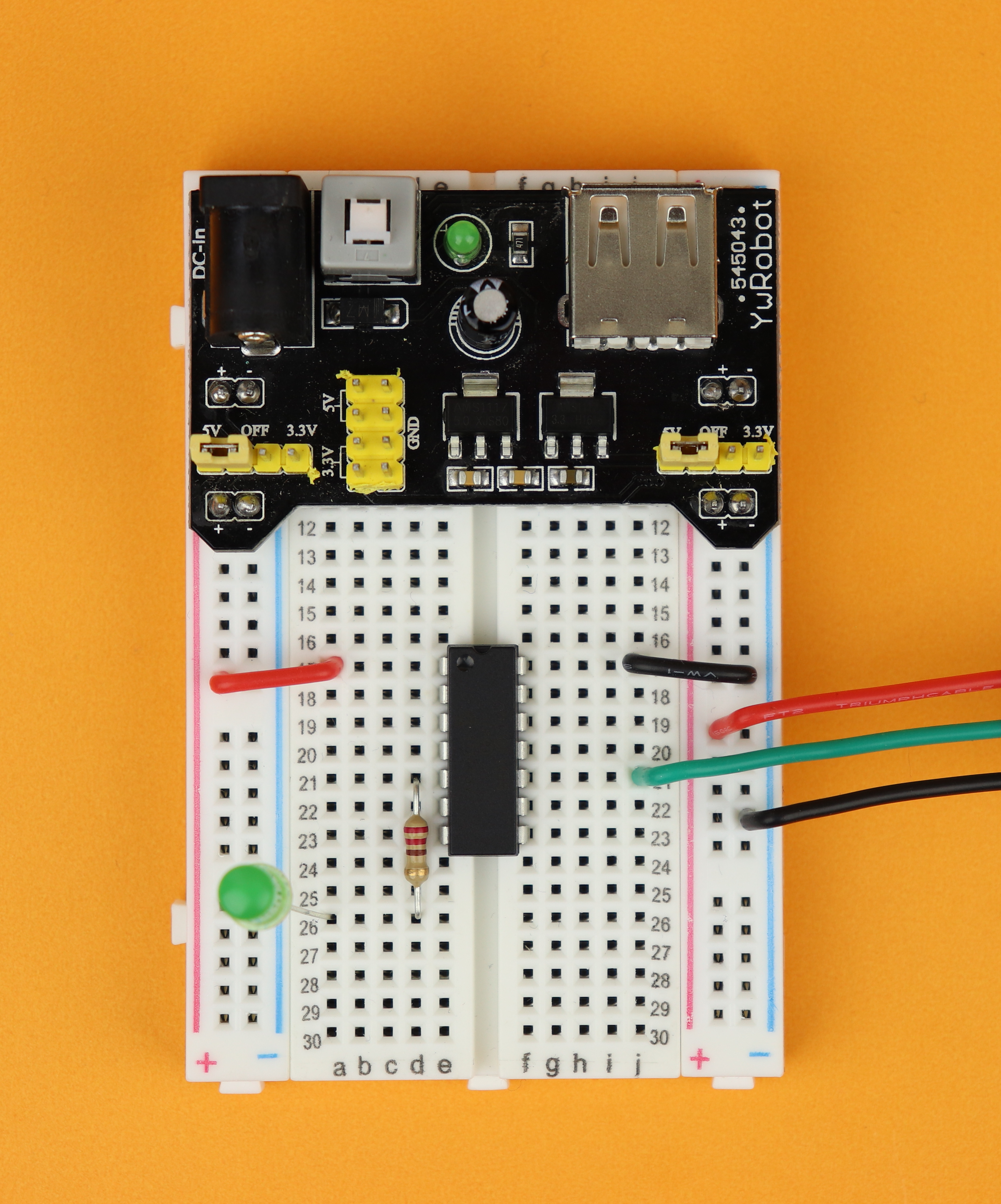
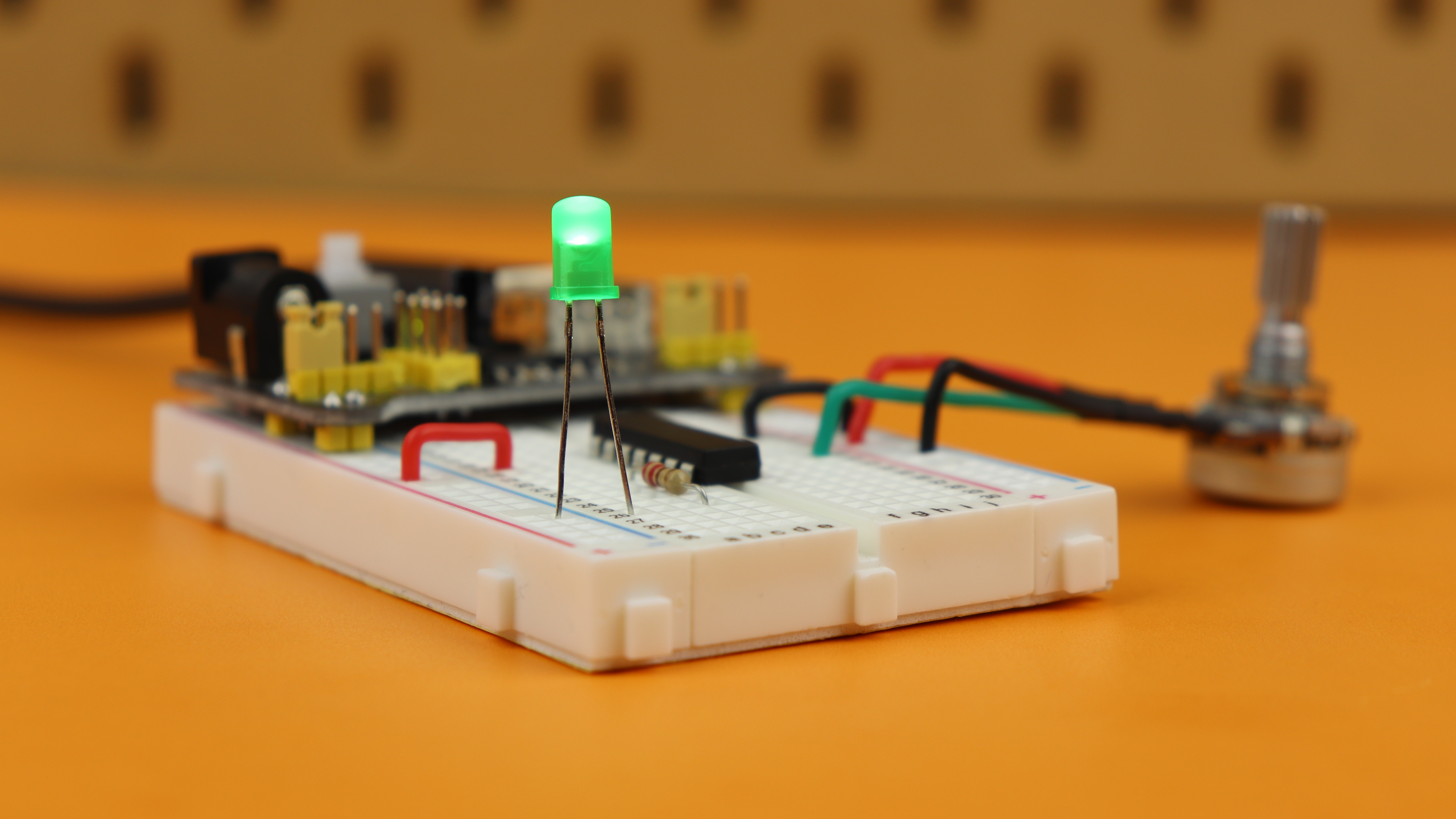
And that's it! You can now plug a standard USB cable into the USB breadboard power supply, and turn the power supply on by pressing the white-greyish button. After that, you can use the potentiometer to adjust the brightness of your LED!
Here is another picture of the finished circuit:
YouTube video
I covered this entire project in a dedicated YouTube video:
Final thoughts?

And here we are! We have understood how we can convert analog signals from the real world into a sequence of 1's and 0's that can easily be digested by microcontrollers. This little tutorial may be a bit boring on its own, granted, but just imagine the possibilities of what we can do with this new knowledge:
- We can have new and interesting input devices with potentiometers.
- We can measure voltages, resistances, brightness, volumes, currents, and all other kinds of analog signals and let our PIC microcontroller react to it!
- Everything that has not a clear 1 or 0 as a value has just become accessible to us!
Thanks for reading this tutorial, and I hope you have found it useful. Please, as always, reach out on social media if something was not clear enough, or if you want to learn more!
Appendix: The full source code
Here you can find the full source code. The code (as well as the .hex file) are also available for download in the resources box.
/*
 * File:   main.c
 * Author: boos
 *
 * Created on January 24, 2020, 05:02 PM
 */

// CONFIG1
#pragma config FOSC = INTOSC    // Oscillator Selection Bits (INTOSC oscillator: I/O function on CLKIN pin)
#pragma config WDTE = OFF       // Watchdog Timer Enable (WDT disabled)
#pragma config PWRTE = OFF      // Power-up Timer Enable (PWRT disabled)
#pragma config MCLRE = OFF      // MCLR Pin Function Select (MCLR/VPP pin function is digital input)
#pragma config CP = OFF         // Flash Program Memory Code Protection (Program memory code protection is disabled)
#pragma config BOREN = OFF      // Brown-out Reset Enable (Brown-out Reset disabled)
#pragma config CLKOUTEN = OFF   // Clock Out Enable (CLKOUT function is disabled. I/O or oscillator function on the CLKOUT pin)
#pragma config IESO = OFF       // Internal/External Switchover Mode (Internal/External Switchover Mode is disabled)
#pragma config FCMEN = OFF      // Fail-Safe Clock Monitor Enable (Fail-Safe Clock Monitor is disabled)

// CONFIG2
#pragma config WRT = OFF        // Flash Memory Self-Write Protection (Write protection off)
#pragma config CPUDIV = NOCLKDIV// CPU System Clock Selection Bit (NO CPU system divide)
#pragma config USBLSCLK = 48MHz // USB Low SPeed Clock Selection bit (System clock expects 48 MHz, FS/LS USB CLKENs divide-by is set to 8.)
#pragma config PLLMULT = 3x     // PLL Multiplier Selection Bit (3x Output Frequency Selected)
#pragma config PLLEN = ENABLED  // PLL Enable Bit (3x or 4x PLL Enabled)
#pragma config STVREN = ON      // Stack Overflow/Underflow Reset Enable (Stack Overflow or Underflow will cause a Reset)
#pragma config BORV = LO        // Brown-out Reset Voltage Selection (Brown-out Reset Voltage (Vbor), low trip point selected.)
#pragma config LPBOR = OFF      // Low-Power Brown Out Reset (Low-Power BOR is disabled)
#pragma config LVP = OFF        // Low-Voltage Programming Enable (Low-voltage programming disabled)

#include

// define clock frequency to be 4MHz
#define _XTAL_FREQ 4000000

void main(void) {

    // set internal oscillator to 4MHz
    IRCF0 = 1;
    IRCF1 = 0;
    IRCF2 = 1;
    IRCF3 = 1;

    // ADC settings

	// ADC sampling frequency per bit is F_osc/16
	ADCS0 = 1;
	ADCS1 = 0;
    ADCS2 = 1;

    // result alignment
    ADFM = 0;

	// RC0 as analog input
	TRISC0 = 1;
    ANSC0 = 1;

    // select channel AN4 (which corresponds to RC0)
    CHS0 = 0;
    CHS1 = 0;
    CHS2 = 1;
    CHS3 = 0;
    CHS4 = 0;

	// turn the ADC on
	ADON = 1;

    // PWM settings

    // PWM1 module is RC5
    TRISC5 = 0;

    // configure TIMER2
    PR2 = 0xff;
    T2CON = 0b100;

    // turn on PWM module
    PWM1EN = 1;
    PWM1OE = 1;

    // main loop
    while (1) {

		// read 10-bit ADC value
        GO = 1; while (GO);

        // set 10-bit duty cycle value for PWM module
        PWM1DCH = ADRESH;
		PWM1DCL = ADRESL;

        // wait a bit
        __delay_ms(1);

    }

    return;

}