CD4017 code lock with wrong code detection
February 28, 2021 • project
Some time ago we learned how to use the CD4017 decimal counter integrated circuit, and in this project we will use it to build an advanced digital code lock with a built-in wrong code detection. This circuit is quite reliable because it detects any wrong code attempts, which also makes this circuit rather unique among all the other CD4017 code lock varieties out there.
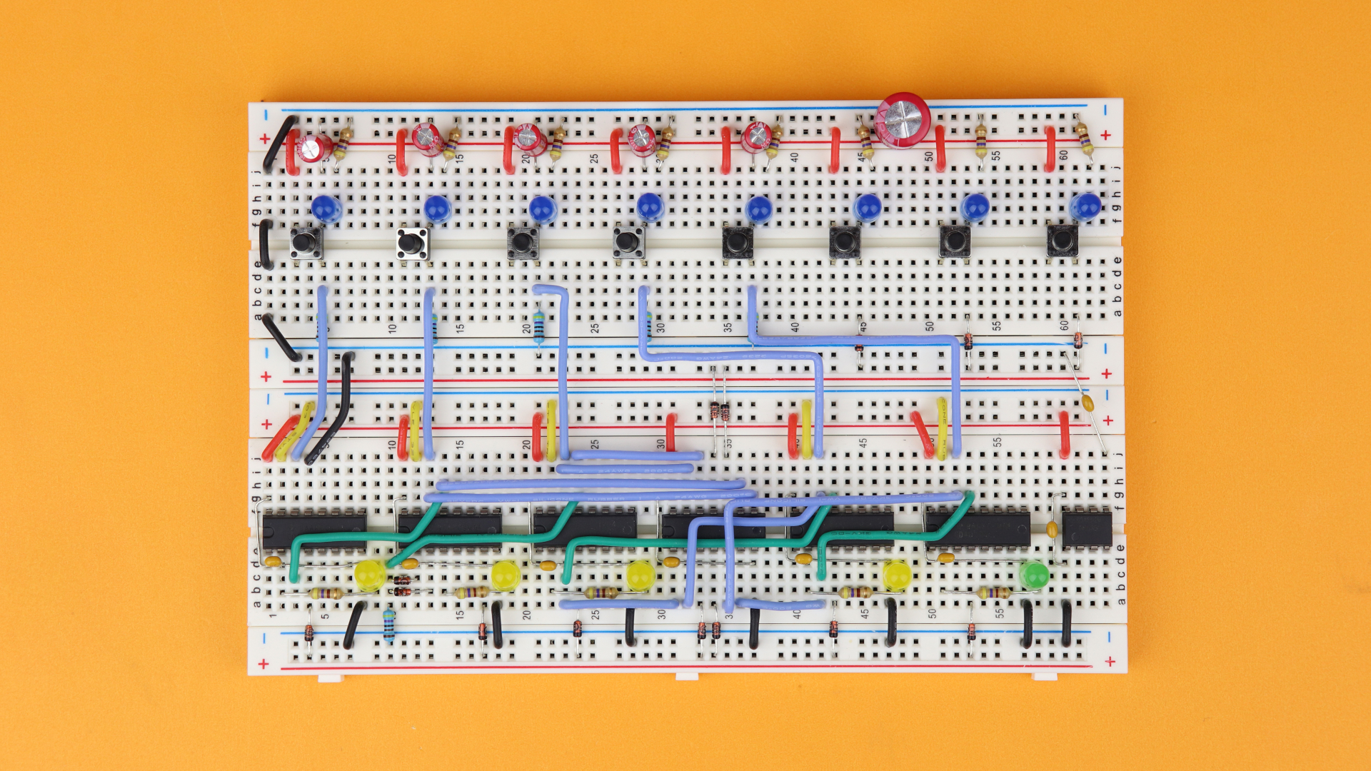
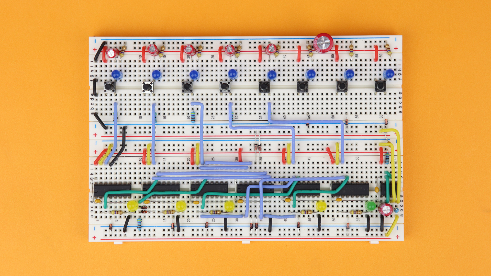
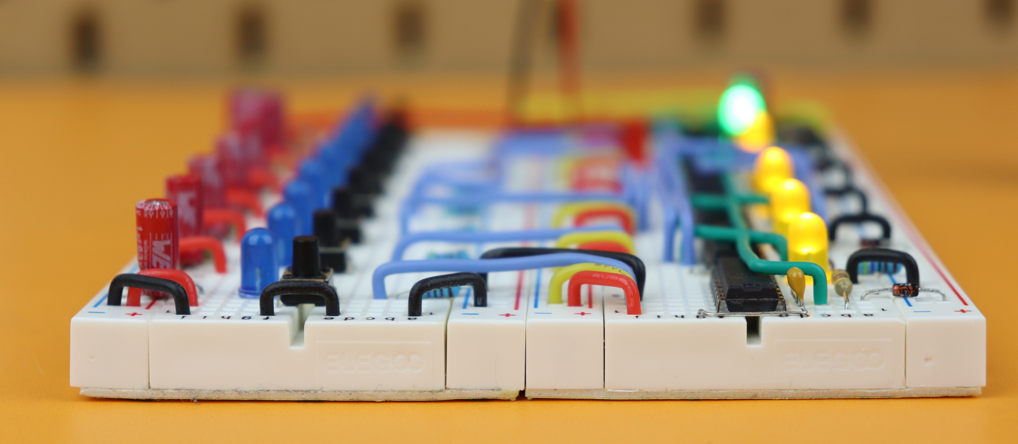
Here you can see a picture of the final code lock:

At the top you can see the keys, and each one has their own LED for fun. At the bottom you can see the CD4017 counters, and four of them have a yellow LED and the last one has a green LED. When you enter the code (here it is A-BB-C-D-E), at each stage one of these LEDs goes on. When the green LED is on, the code lock is unlocked. Whenever you enter a wrong code, the red LED blinks on and resets the code lock, and you could use that for an alarm function.
As you can see there is quite a lot going on, but as always we will go through all steps together so that you can build this code lock yourself. So let's get started!
What you need
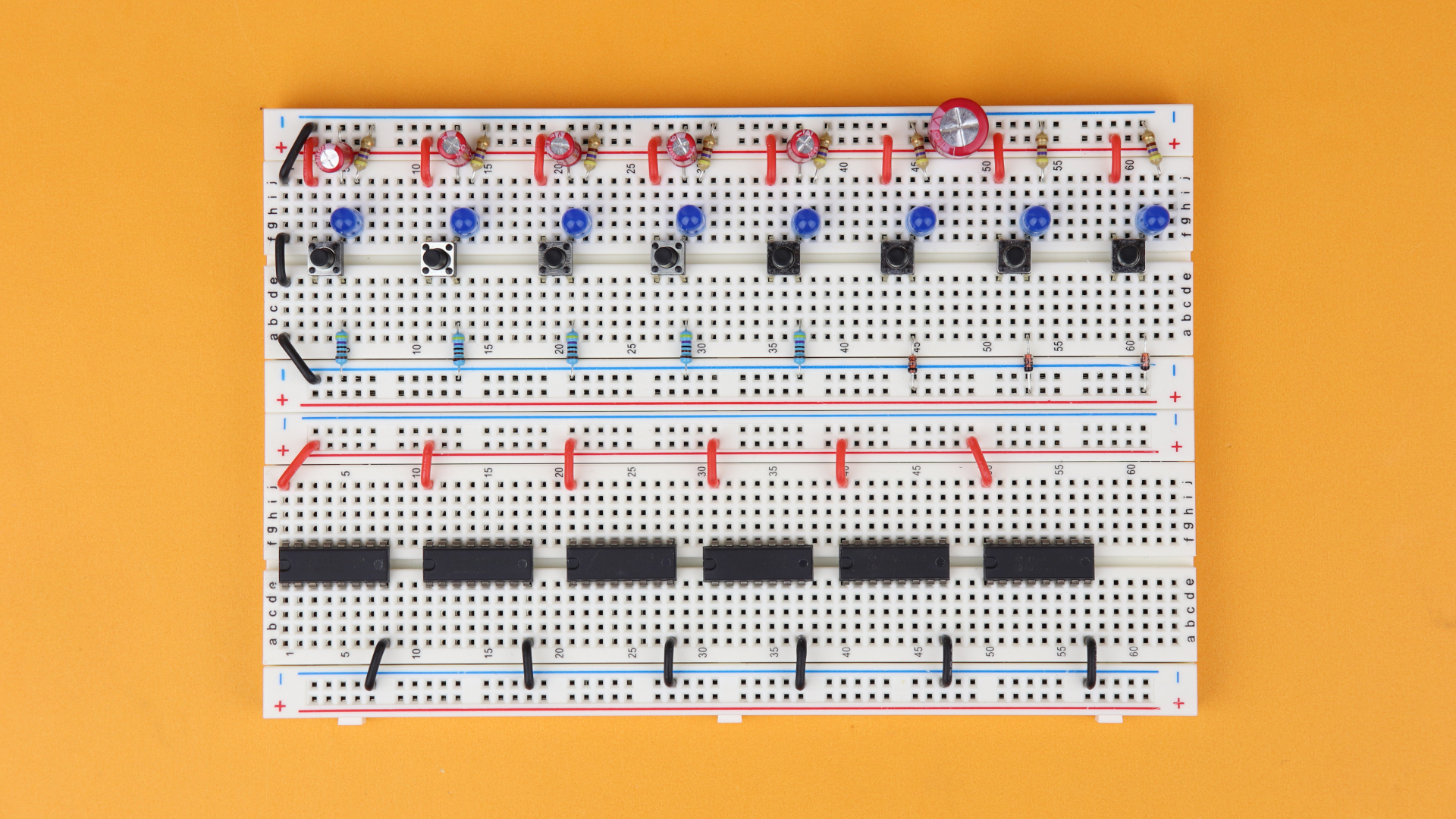
Here is a picture of what you need if you want to follow along with this project:
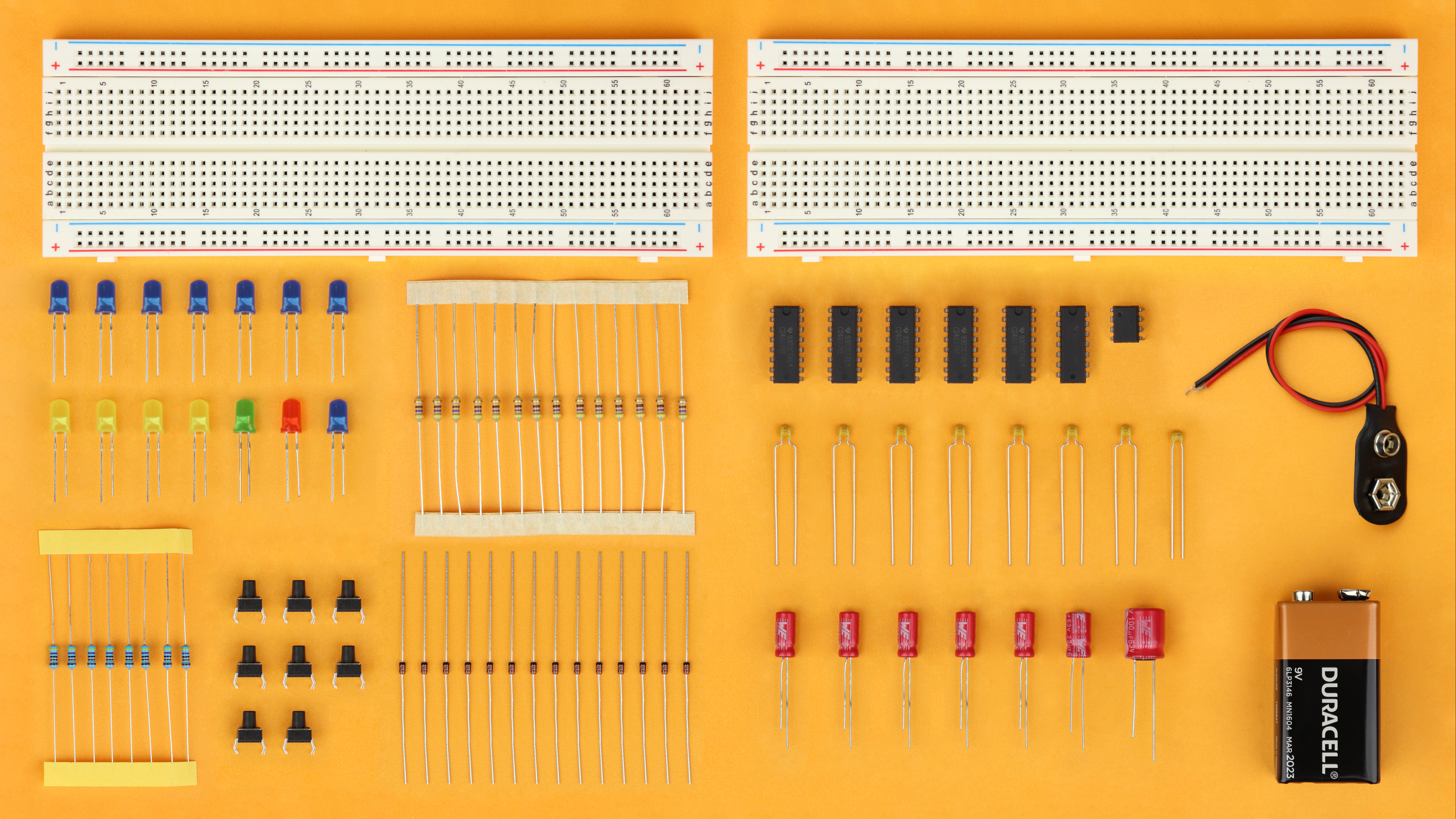
As always there is a detailed list of all components on the side of this article (desktop version) or at the bottom of this page (mobile version). Besides breadboards, resistors, LEDs, pushbuttons, and capacitors, this project makes use of the following key components:
- CD4017: we are building a 5-digit code lock, so we need 5 CD4017 decimal counter chips.
- CD4081: this quadruple AND gate is required for the wrong code detection.
- NE555: we use the NE555 timer for a stable reset circuit.
- 1N4148 diodes: these diodes work as OR gates, more on that later.
But don't worry, we will get into a lot more detail below.
CD4017 in a nutshell
This projects uses many key features of the CD4017 decimal counter. If you already know how the CD4017 works, you can skip ahead to the schematic (or check out our detailed tutorial if you are new to the CD4017). If you are in a hurry, here is a brief summary:
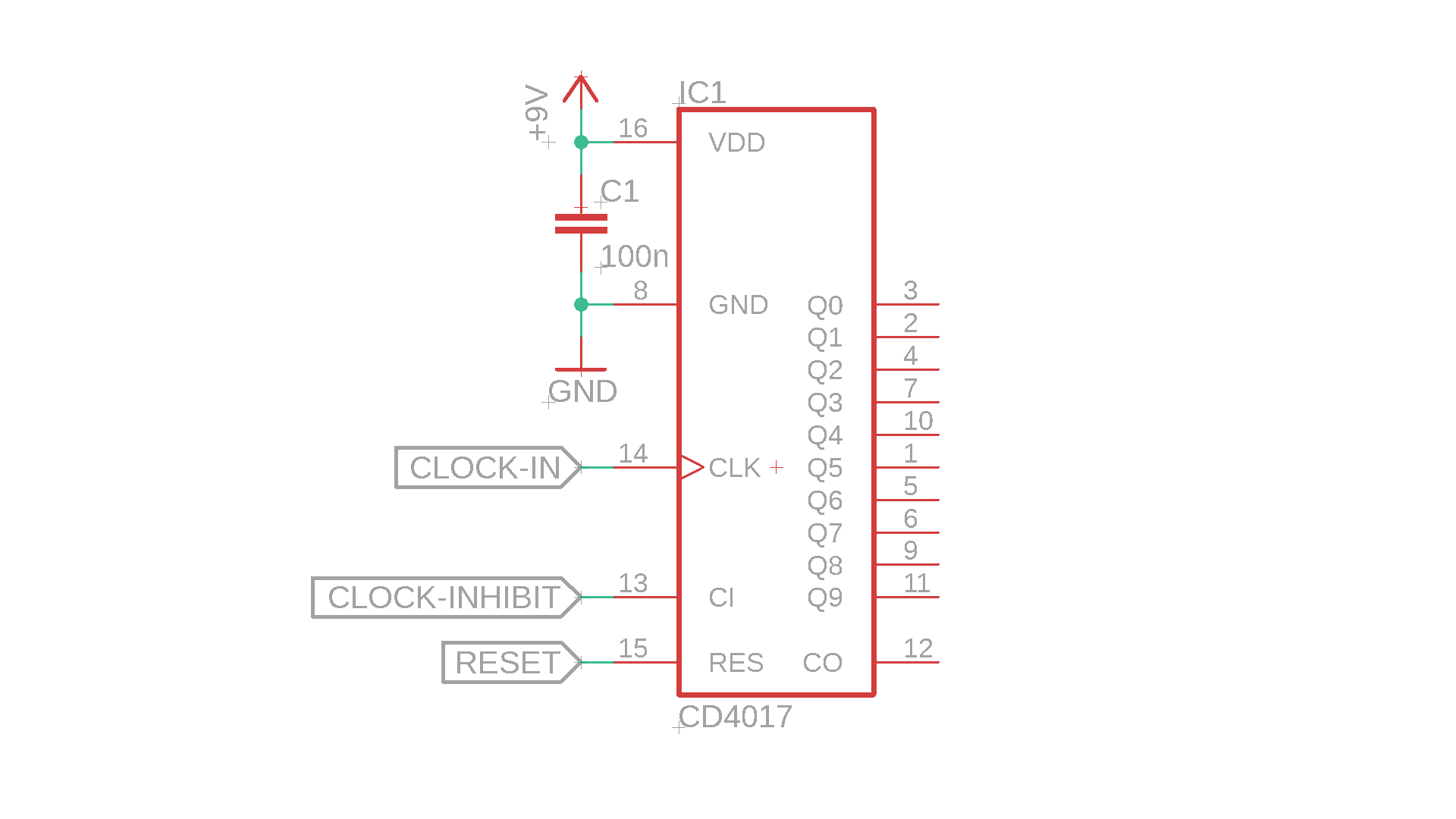
The CD4017 is a decimal counter from 0 to 9. It runs between 3V and 18V DC, and it is always suggested to add a 100nF bypass capacitor (C1 in the picture above) close to the chip. Here we won't run it at very high frequencies, so it is probably not necessary, but it doesn't hurt either. Here is what the pins of the CD4017 do:
- Q0–Q9 are the outputs and represent the current value of the counter. The active output is at VDD (“high”), and all inactive outputs are at the GND level (“low”).
- CLK is the clock input, and the counter increases by one after a positive pulse on this input.
- CI is the clock inhibit input. When it is tied to ground then the counter works normally, but whenever it is connected to VDD the counter ignores all clock pulses. This pin is very important for this project.
- RES, well, resets the counter back to zero whenever a positive pulse is applied to this input.
- When increasing the counter past 9 it resets back to 0 automatically, and when that happens it also sends out a positive pulse on the CO (carry out) pin. We don't use this pin in this project.
If any of that confuses you: no worries, we have you covered! Check out the CD4017 tutorial :)
Schematic
And now we are ready to look at the schematic for our code lock, here it is:
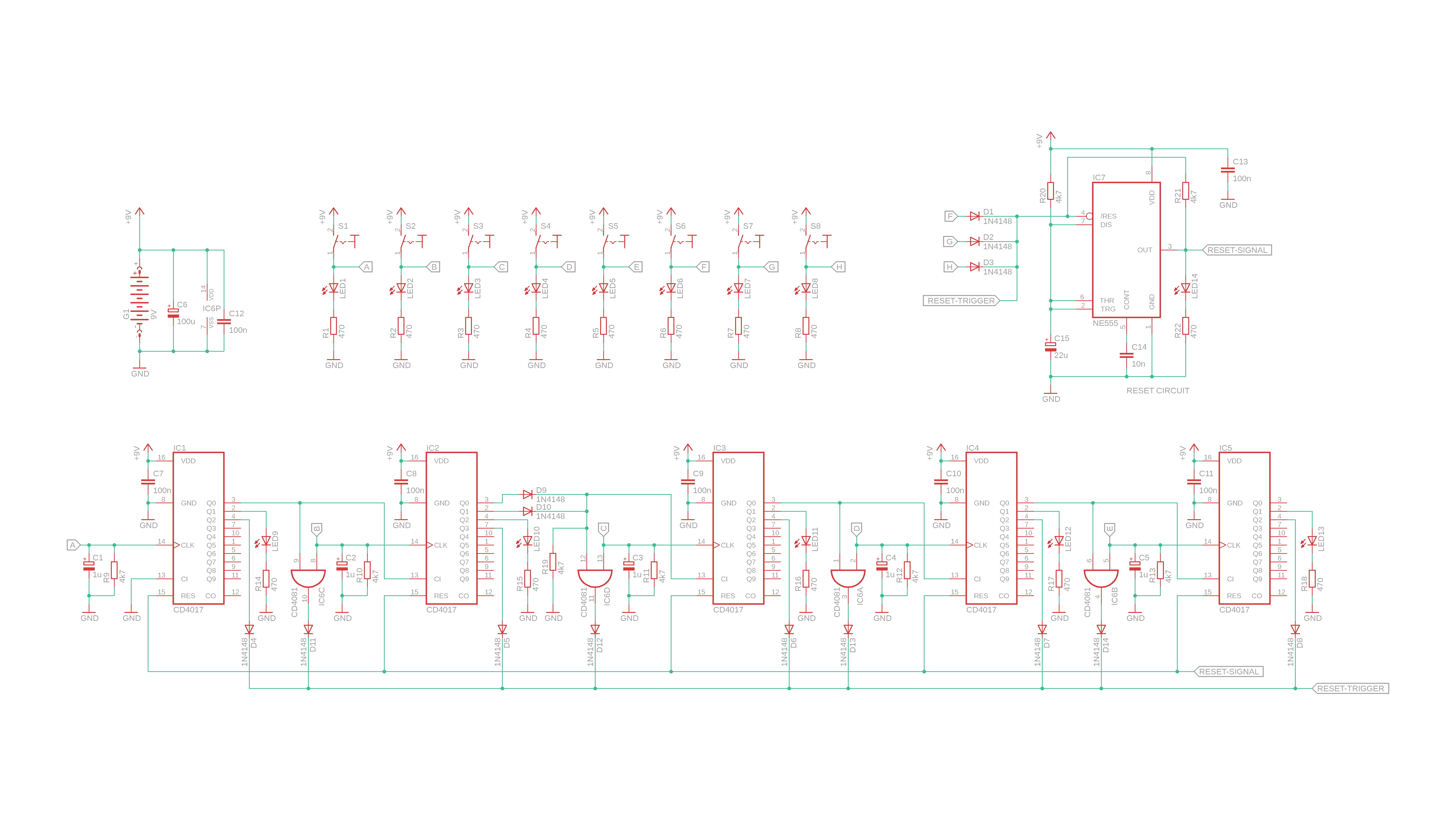
I know, I know, it's a lot to take in. So let's highlight the separate pieces:
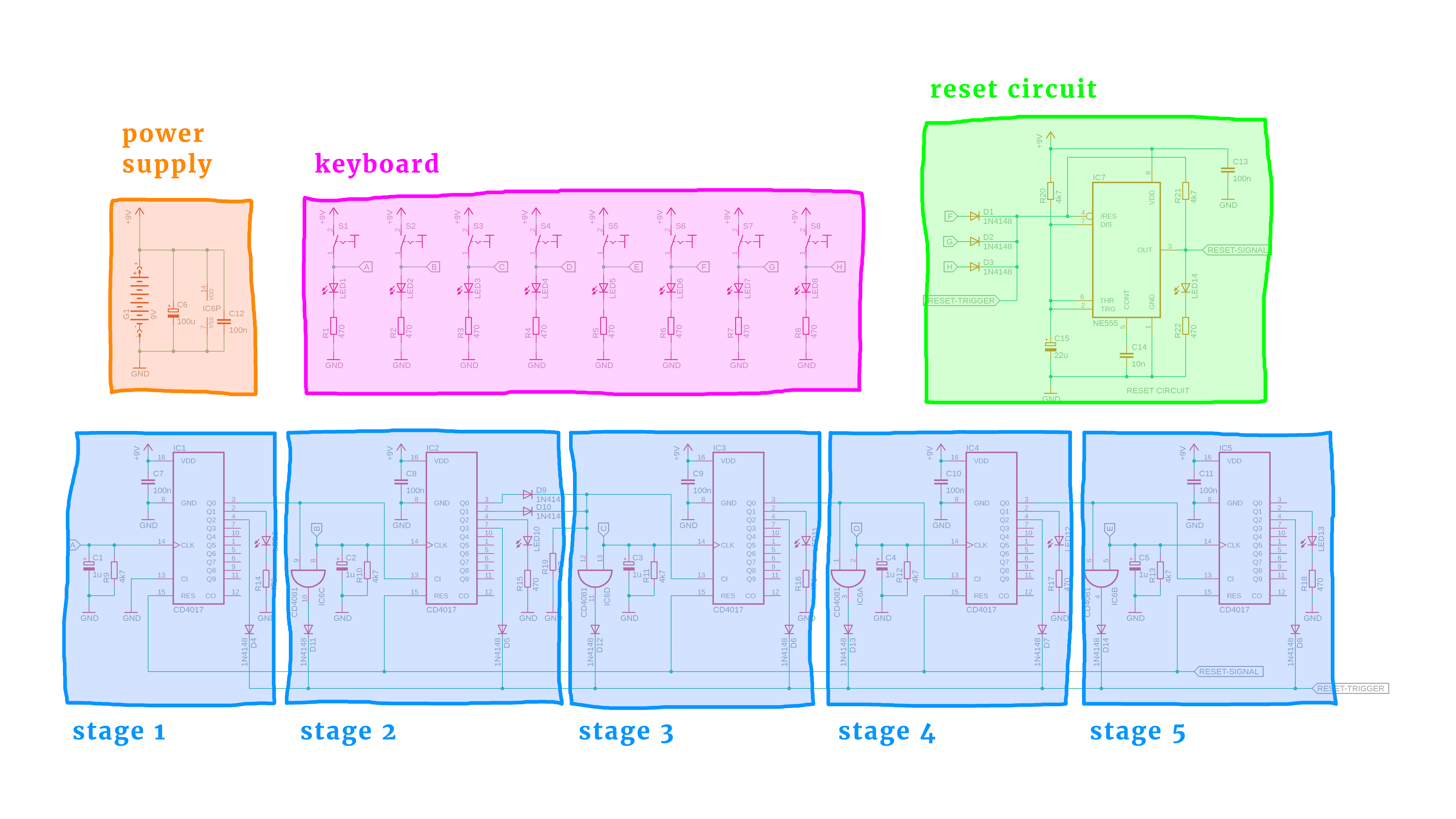
(You can click on the schematic for a larger view, and go back and forth between the bare schematic and the highlighted version, using your arrow keys.)
In a nutshell, the circuit works like this: using the keyboard you enter the code A-BB-C-D-E, which unlocks the code lock, and LED13 turns on. If you enter a wrong code, then the circuit resets (via the reset circuit) and the alarm LED (LED14) turns on and off. You could use that LED to trigger an alarm, or you could even connect it to another counter that keeps track of the wrong code attempts and triggers an alarm after a specified amount of wrong codes.
So let's dive into the details! First, let's talk about the power supply, the keyboard, and the reset circuit, because they are quite simple:
- The power supply is a simple 9V battery, with a 100μF bulk capacitor in parallel. This power is connected to all integrated circuits in the schematic. The funny looking symbol IC6P represents the power supply for IC6, and C12 is its 100nF bypass capacitor. All other integrated circuits (the five CD4017's and the NE555) are also connected to the power supply, each with their own 100nF bypass capacitor as well.
- The keyboard is very simple, too: it has eight pushbuttons that light up an LED whenever they are pressed. These buttons are used to input your code, and you can add as many buttons as you like. I just used eight here because they fit nicely on a breadboard. I also added LEDs to make it look more interesting whenever a button is pressed, but the LEDs are not necessary for the circuit to work, so if you don't like them you can just forget about them. And last, the symbols A–H are labels that we use in the lower part of the schematic: this way we don't have to draw connections from the top to the bottom which would make the schematic harder to read. Later on the breadboard we will connect all labels of the same name together. (Also, if you are new to reading schematics, check out our schematics 101 article if you want.)
- And last: the reset circuit. We use it to generate a stable reset signal for all the counters in this circuit. It works like this: even a very short pulse on the label RESET-TRIGGER will generate a fixed-length reset signal at the aptly named label RESET-SIGNAL of around 70ms. This makes sure that the reset signal is on long enough so that all counters have enough time to reset properly. If only one counter would not reset reliably, then the entire circuit would not work, so yeah: this is important. If you want to learn more about the reset circuit, check out the relevant part in our detailed article on the CD4017 :)
In this project we wire the keys A, B, C, D, and E to the five stages at the bottom (more on that later). The unused keys are directly connected to the reset trigger input, because they should reset the code lock whenever they are pressed. For each unused key we need to insert a diode (D1–D3). Why? This is because of the LEDs. If we press, say, F, then LED6 would light up, as it should, but also LED7 and LED8. And this would immediately give away all keys that are not part of the code, which would be a security risk. So, yeah, these diodes are important :)
Okay, but how does the actual code lock part work? Our code is A-BB-C-D-E, and you can easily change the circuit to have codes like H-D-A-B-GG, B-D-H-E-F, BB-A-CCCC-D-EE, and so on. The only codes you cannot generate with this circuit are codes like A-B-A-D-E, or A-B-C-BB-E, where some keys are repeated in separate groups. But on the flip side, wrong code attempts are always caught, so this code lock is 100% secure.
The circuit I am showing you here is set to the code A-BB-C-D-E. I think of this code as of five groups, so we need five CD4017 counters. In the colored schematic above you can see five stages at the bottom that correspond to the five groups of the code. Each group of the code unlocks one stage, and they have to be unlocked in the exact right sequence, otherwise the circuit resets. So, pressing A unlocks stage 1, pressing B twice unlocks stage 2, pressing C unlocks stage 3, and so on.
So to understand how the code lock works it's a good idea to imagine what happens when you enter the correct code, A-BB-C-D-E. Let's do that first, and later we will look at what happens when we mess it up and enter the wrong code.
Entering the right code A-BB-C-D-E:
- Alright, step 0 happens immediately after you plug in power: the reset circuit triggers once and resets all counters. This is very important because it creates a reliable starting point. So, to begin with, all counter outputs are set to 0, which means that all Q0 pins are high and all other outputs Q1–Q9, for all counters, are low. Because all Q0 pins are high, all clock inhibit pins are high, too, except for the first one, meaning that all stages except for the first one are locked and disabled after power-up.
- Let's have a look at the first counter, IC1. At the clock pin, R9 works as a pulldown resistor that holds the clock input at low level whenever the pushbutton is not pressed. And the capacitor C1 is a debouncing capacitor that we need for mechanical switches to work reliably, check out the CD4017 tutorial for more on that. The clock inhibit input of IC1 is permanently held low, so that any clock pulse is registered and the counter increases from 0 to 1.
Now we press A. The counter IC1 increases and Q0 is low, and Q1 is high. LED9 turns on and shows us that the first stage is ready.
(And yes, that makes the circuit not very secure, because you can see immediately if you pressed a correct key or not. So in a real world application you should probably not include the intermediate LEDs LED9–LED12. I put them in the project only to make it look more interesting and easier to understand what is going on.) - Alright, so stage 1 is done and Q1 is high. This means that now the clock inhibit pin of IC2 is low, which activates stage 2 so that it can react to clock pulses. So let us press B. What happens?
The second counter increases from 0 to 1 so that Q0 goes low, and Q1 goes high. But we're not done yet with stage 2, because the two diodes D9 and D10, together with R19, work as an OR gate and still disable stage 3: if either Q0 or Q1 is high, then the clock inhibit pin of IC3 is held high.
So we have to press B again, and then the counter increases a second time from 1 to 2. Now, Q1 goes low and Q2 goes high. This turns on LED10, stage 2 is complete, and stage 3 is activated and ready to go!
(And if you wanted the code lock to instead require four presses of B then you could simply add two more diodes on Q2 and Q3, you get the idea.)
But back to entering the code. Stage 3 is activated and waits for us. - Now, when we press C, counter 3 increases from 0 to 1 and LED11 goes on, and that activates stage 4.
- And then, pressing D increases counter 4 from 0 to 1, which turns on LED12 and activates stage 5.
- And then, pressing E increases counter 5 from 0 to 1, which turns on LED13. At this moment the code lock is unlocked, and pressing any key will reset it back to the standby mode. So, if you want anything special to happen when the code lock is unlocked, then connect it to the output Q1 of IC5 in parallel to LED13 :)
So you see, it is basically the same idea just repeated over and over and over again. And using diodes allows us to have multiple key presses in one group, which is also the main reason why I used the CD4017 counter for each stage instead of a flip flop.
And now that we understand this, let's imagine we enter the wrong code. What is different?
Entering the wrong code:
So here is a very simple case first:
- If you press any key that is not part of the code (here that would be F, G, or H) then the code lock resets immediately because these keys are connected directly to the reset trigger.
But the true challenge lies in also firing an alarm when part of the code is right, and then something goes wrong later. Let's say we put in A-BB-C correctly, so imagine going through the steps 1-3 from the list above, but then we mess it up by not pressing D next (which we should) but E instead.
- That's where the AND gates come in, the symbols IC6A–IC6D in the schematic above. And if you press E, then the AND gate IC6B at the very right kicks in.
Why? Because stage 5 is not active yet, counter 4 is still at 0, which sets the first input of the AND gate to high. But then, pressing E sets its other input high as well. With both inputs of the AND gate high, its output goes high as well, and that resets the code lock because the output of the AND gate is connected to the reset trigger. Which is connected to the reset circuit. Which resets the circuit :)
And it works exactly the same way for all the other keys that are part of our code A-BB-C-D-E. When they are pressed and their stage is not ready yet, their AND gate kicks in and resets the code lock.
Now there is one case that we haven't talked about yet. Imagine you enter A-BB-C correctly, and then press C another time. What happens then?
- Because stage 3 is active, the counter increases and LED11 goes off. But then Q2 goes high, and Q2 is connected to the reset trigger, and that resets the entire circuit.
So you see: all possible wrong combinations are caught by our circuit, giving us 100% reliability :)
And why are there so many diodes?
This project uses 14 diodes, and so far we have only talked about a few of them (D1–D3, as well as D9 and D10). What about the rest? Good question, I am glad you asked :)
You see that all of the remaining diodes that we haven't talked about yet (D4–D8, D11–D14) are connected to the reset trigger rail. This is to protect the outputs of the counters and the AND gates from current flowing into them whenever the reset trigger rail is high. Say, for example, that the output of the AND gate on the left (IC6C) goes high. If the diodes D4–D8 and D11–D14 were not there, then this current would flow into the outputs of the other AND gates, and into the outputs of the five counters. But because they are outputs, a current flowing into them would damage the chips. The diodes prevent that from happening because they don't let the current through in that direction: they are protection diodes.
Okay, so that was the main idea of the code lock. I hope it makes sense. If something in here is very confusing please let me know on social media and I will do my best to improve the article :)
Building the circuit
We will build this circuit on two 830-pin breadboards, and because the schematic is rather involved let's make sure we are on the same page before we begin with the knitty gritty construction :)
Usually, breadboards have two power rails on either side of them:
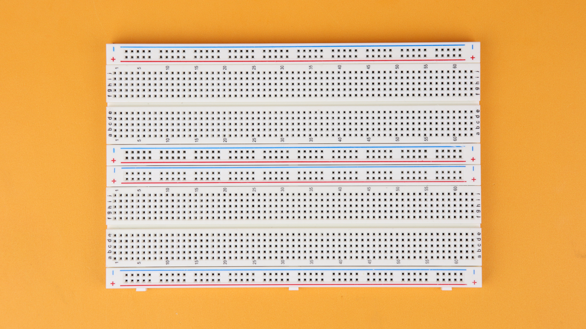
That means we have eight rails in total, quite a lot. Usually these rails are used for the operating voltage of the circuit, which is why the red one has a plus sign and the blue one has a minus sign next to it. But it is a bit of a wasted potential in our project here to use all eight rails for power supply purposes only.
So I thought it would be a good idea to also use some of these rails as the reset trigger rail and the reset signal rail. This way we can make our life a lot simpler because we have to use less wires during construction. Here is the idea in color:
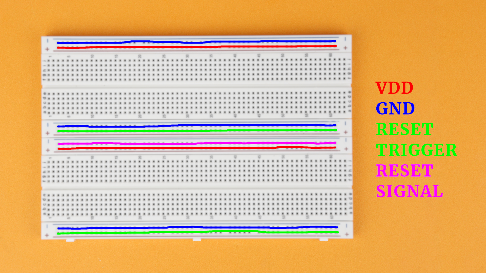
So you see, some of the rails are used as power rails. But the lower + rail of the upper breadboard and the lower + rail of the lower breadboard will be wired as the reset trigger rail, and the upper - rail of the lower breadboard will carry the reset signal. I tried around for quite a bit and this wiring turned out to be the best one for our project :)
And last, be aware that there are two types of 830-pin breadboards. Those with separate power rails, and those with connected ones:
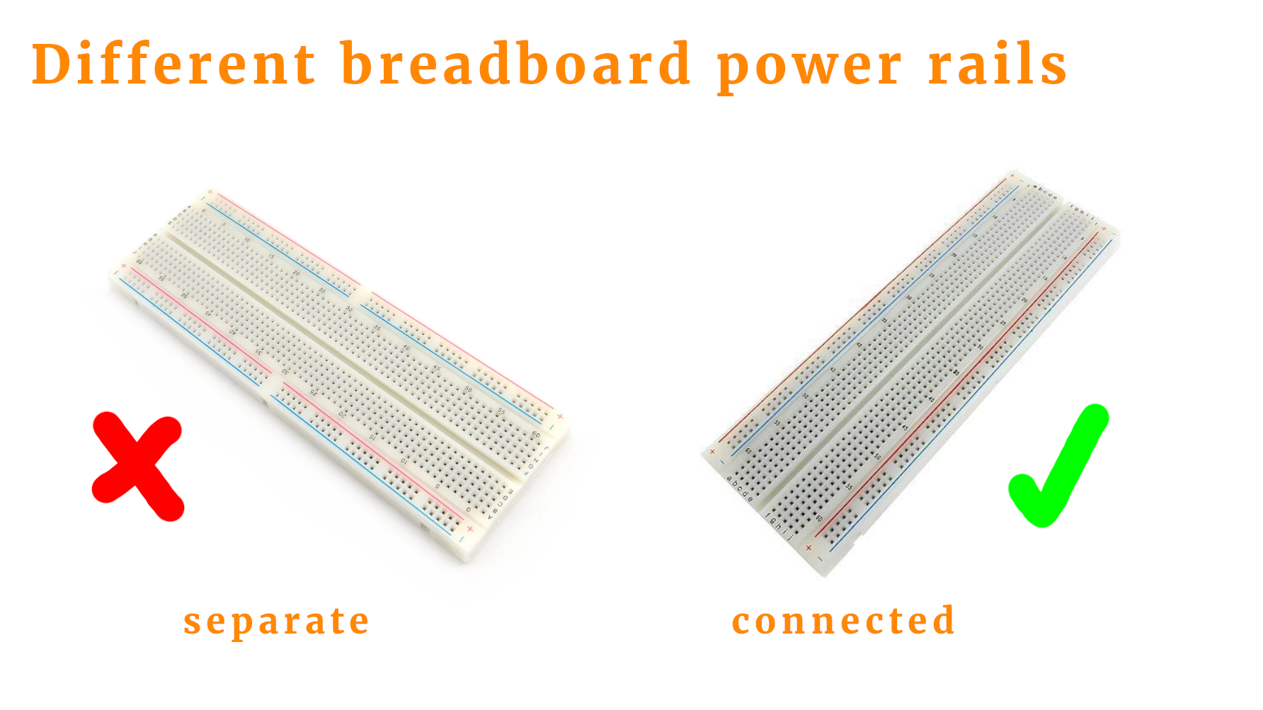
If you use the left type, no worries! Just make sure to insert extra connections in the middle around row 32 so that the rails are connected all the way through from top to bottom. But in this article I will use the already connected breadboard version (right side).
And with that out of the way, let's start building the circuit!
-
-
Step 1
Place two 830-pin breadboards in front of you and connect them together. Make sure that for both of them row 1 points to the left. Electrically it does not matter, but in the following steps we will use the row numbers that result from that orientation.
-
-
Step 2
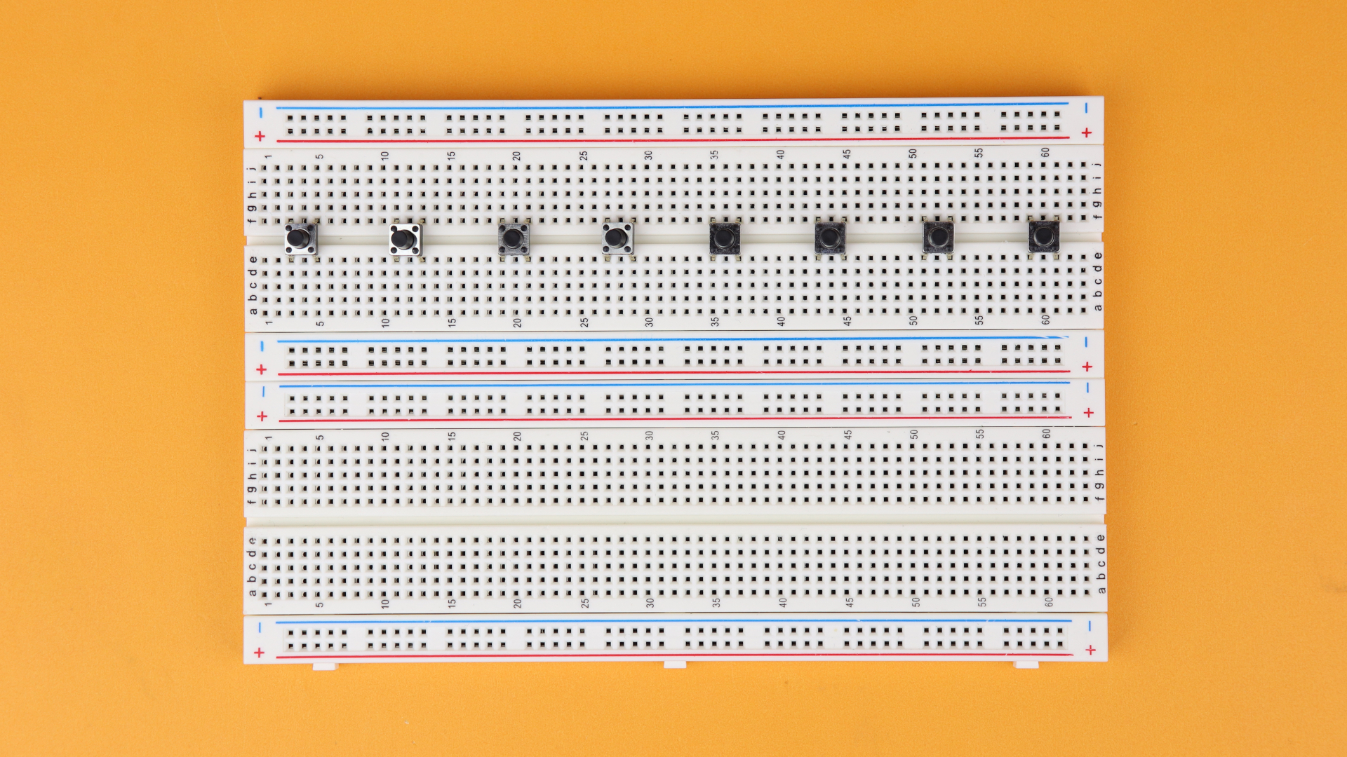
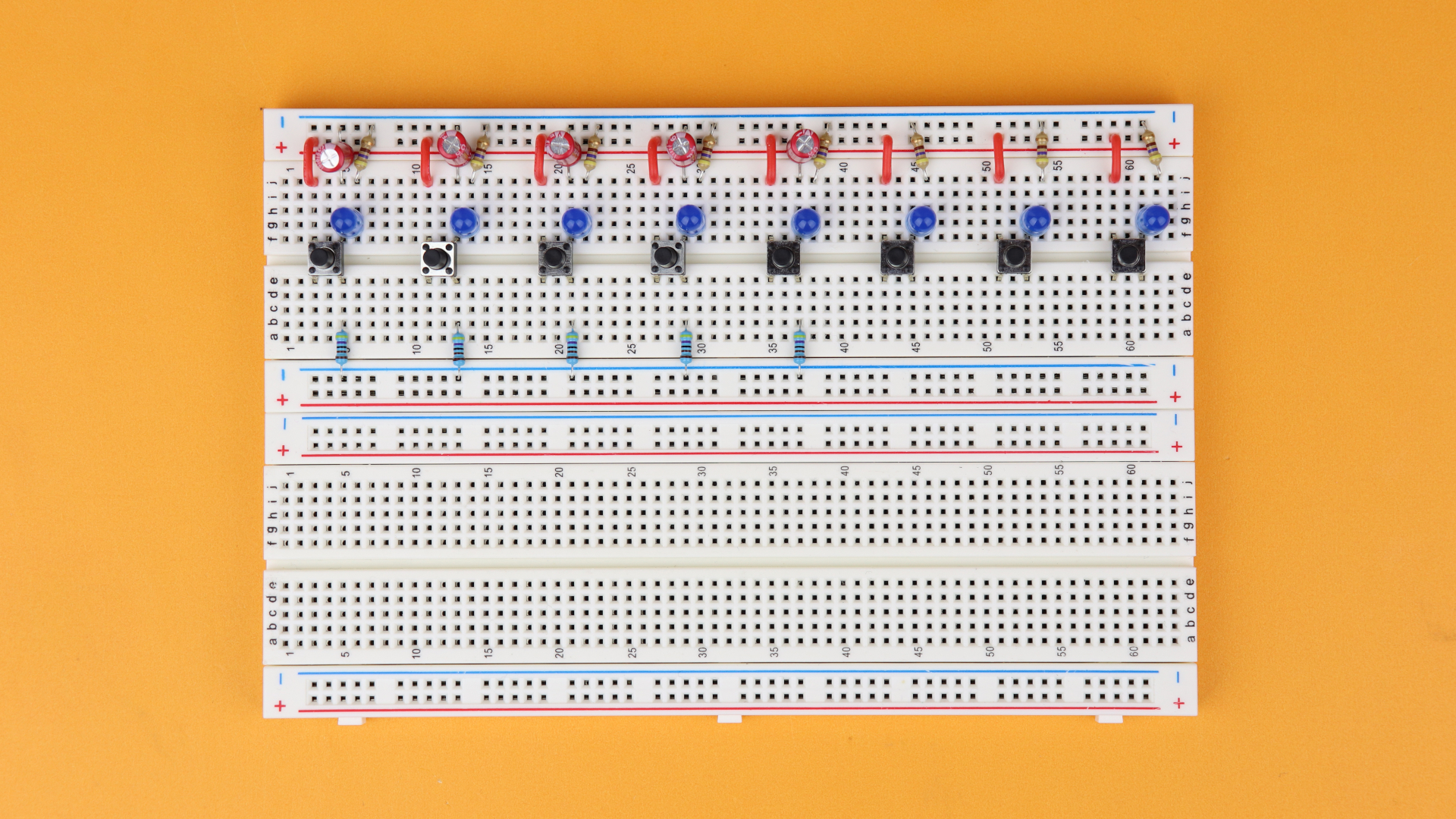
Insert the eight pushbuttons S1–S8 in rows 3, 11, 19, 27, 35, 43, 51, and 59.
-
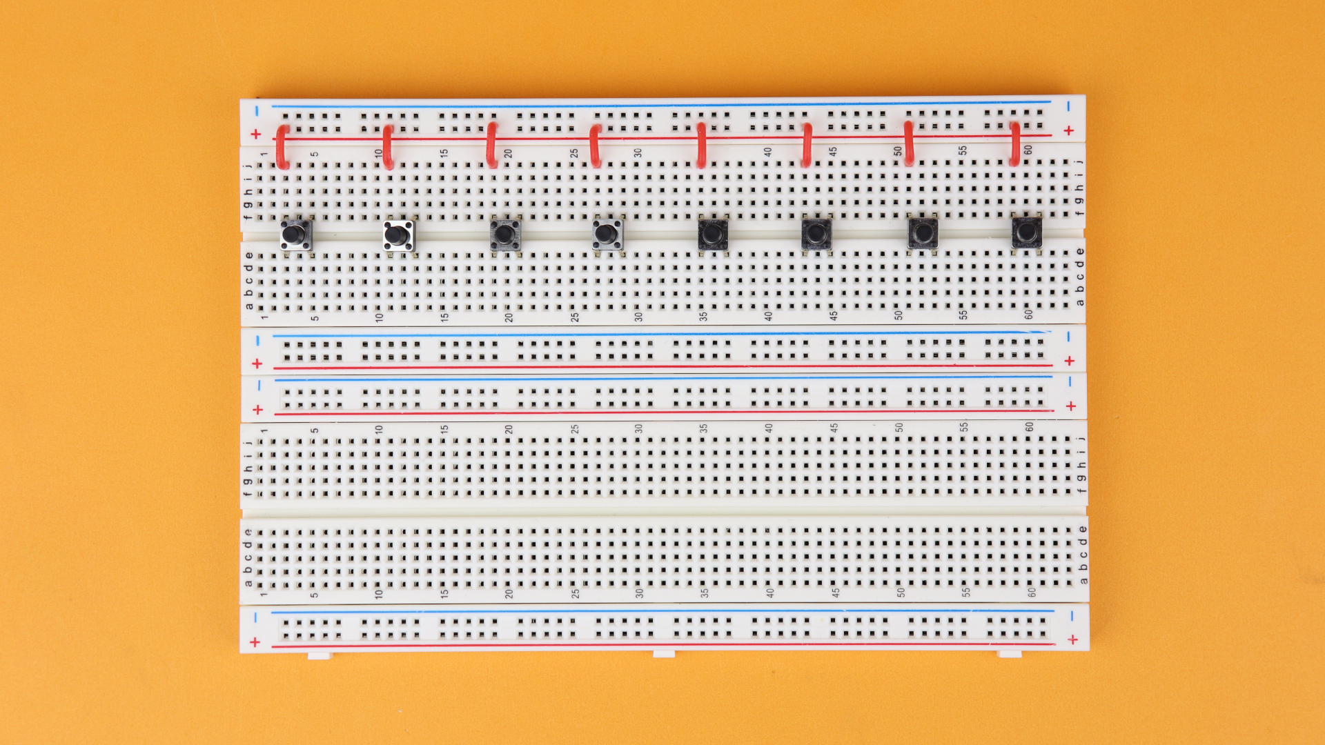
-
Step 3
Connect their upper left terminals to the positive power rail.
-
-
Step 4
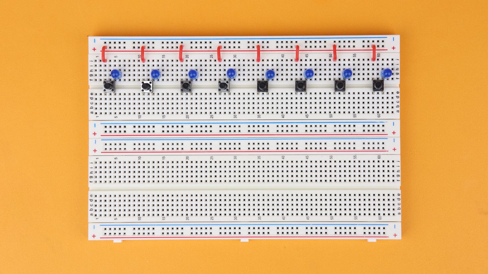
Insert LED1–LED8 above the right terminal in column g, with their cathodes pointing to the right.
-
-
Step 5
Connect their cathodes to the negative power rail with the 470Ω resistors R1–R8. Insert them as shown in the picture, even if they look a bit crooked, because we need the space.
-
-
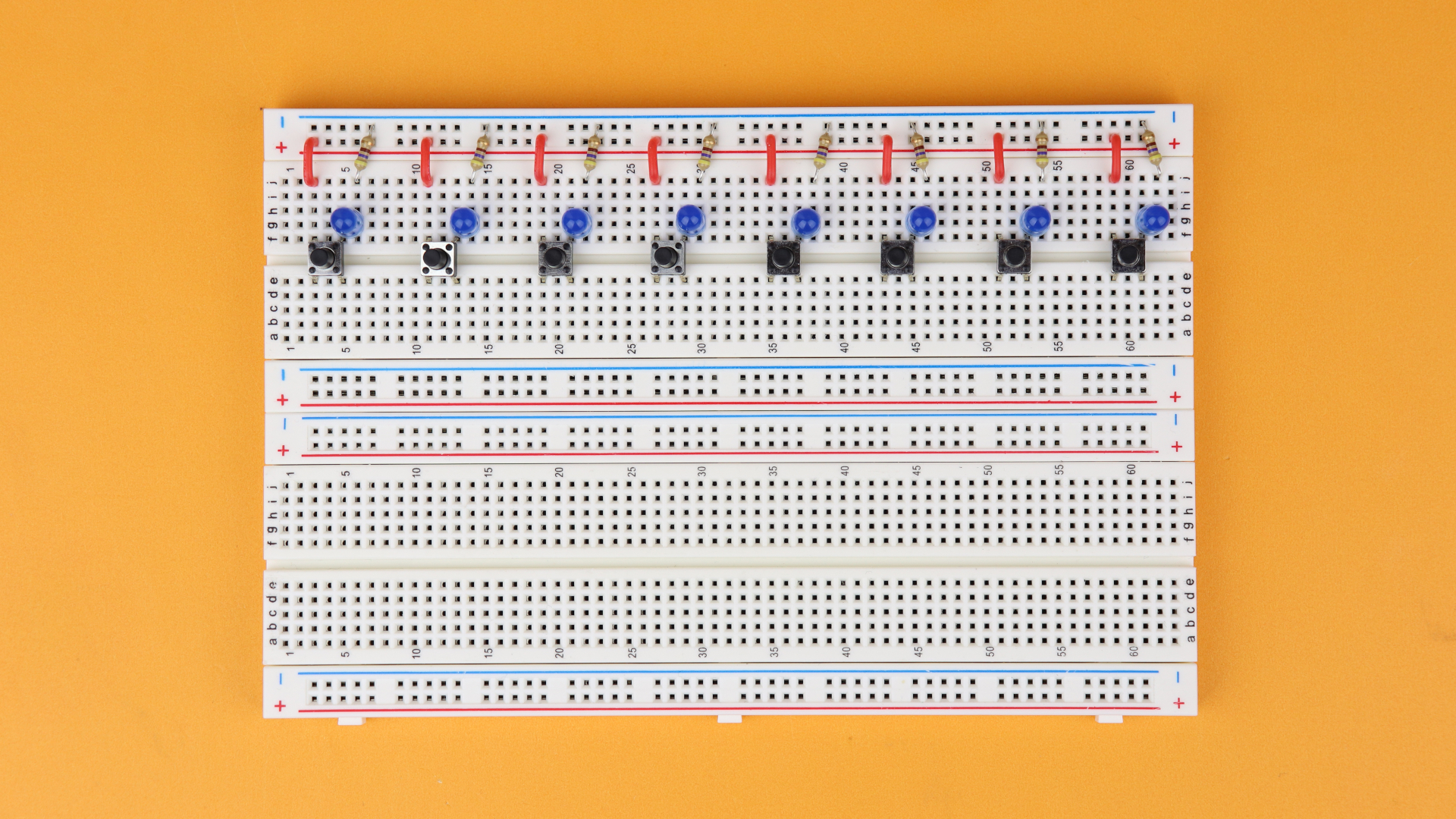
Step 6
Insert the 4.7kΩ pulldown resistors R9–R13 between the right lower terminals of the pushbuttons and the lower ground rail.
-
-
Step 7
Next, place the debouncing capacitors C1–C5 between the upper right terminals of the pushbuttons and the upper ground rail. Important: make sure that the negative terminal of the capacitors, marked with a big minus sign, is connected to the negative power rail.
-
-
Step 8
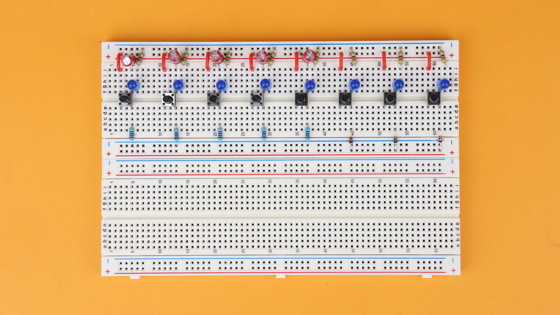
The diodes D1–D3 are next. Connect the right terminal of the remaining three pushbuttons S6–S8 to the lower VDD rail. Important: make sure that the diodes' cathodes (the black rings) are connected to the lower VDD rail. Also keep in mind that the “lower VDD rail” is not actually used as a VDD rail on this breadboard, but rather as the “reset trigger” rail.
-
-
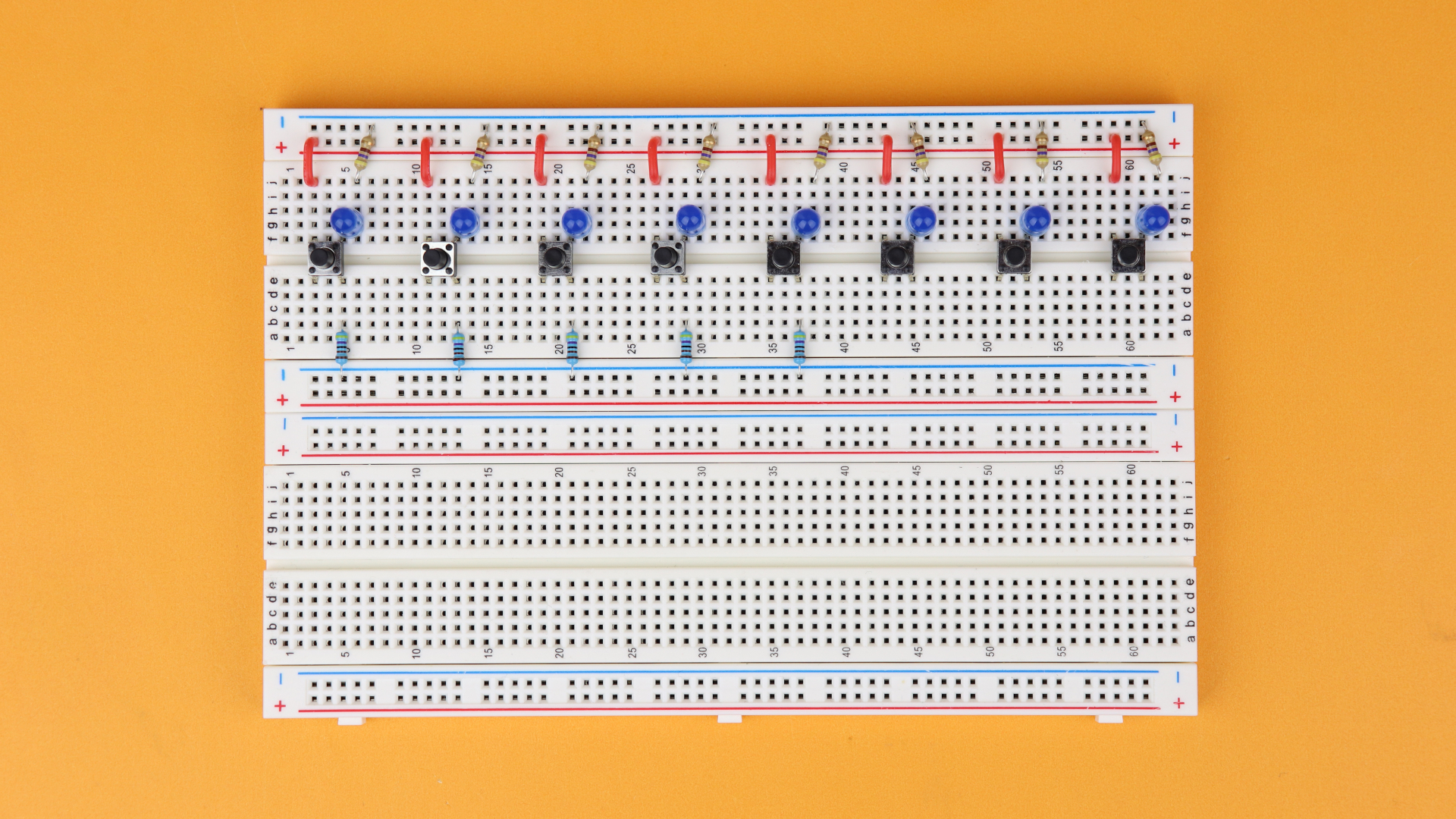
Step 9
Connect the upper and lower ground rails on the upper breadboard and insert the 100μF bulk capacitor C6 in the power rail. Important: make sure that you plug it in correctly with its negative terminal plugging into the blue ground rail, and its positive terminal plugging into the red VDD rail.
-
-
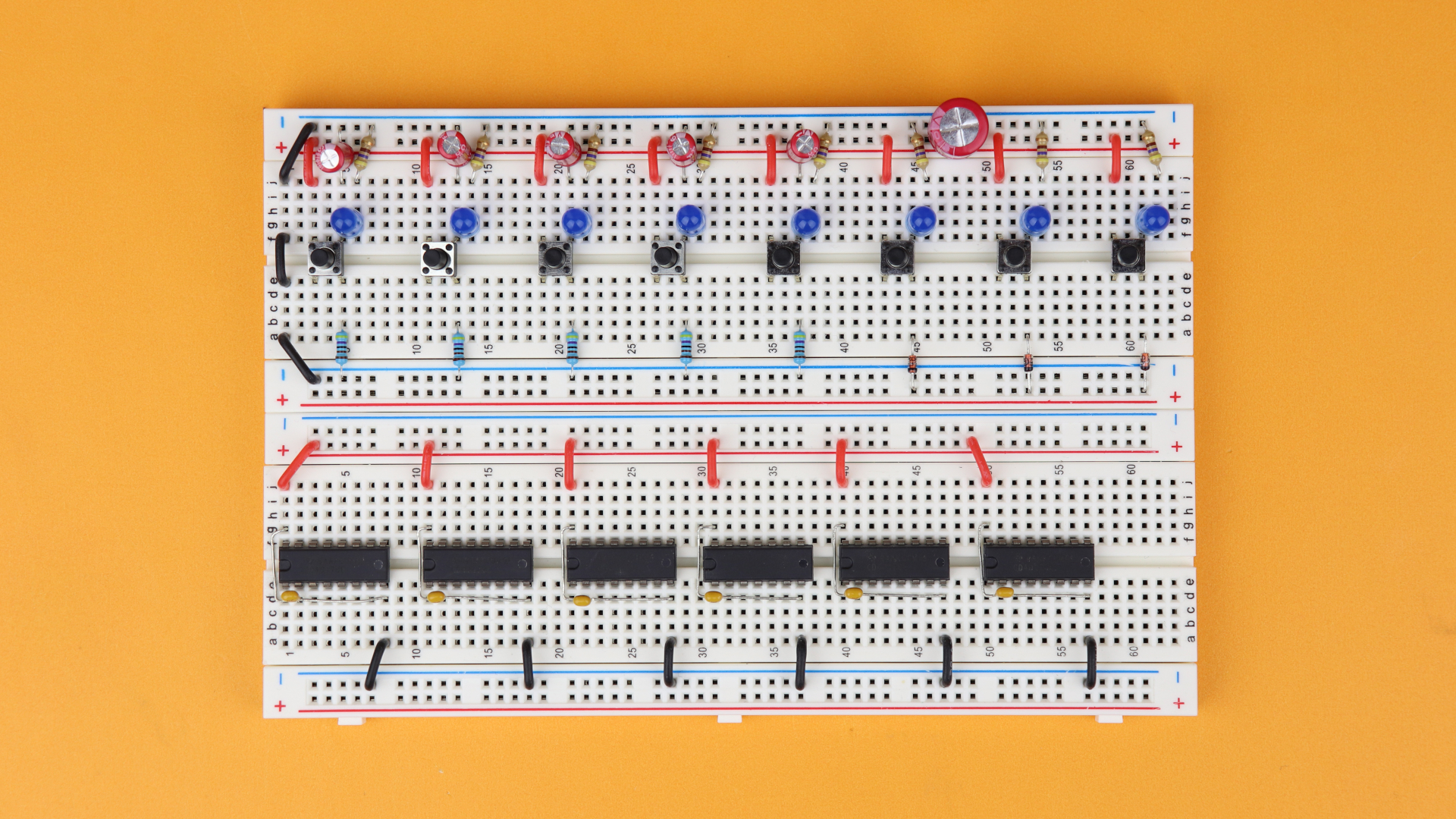
Step 10
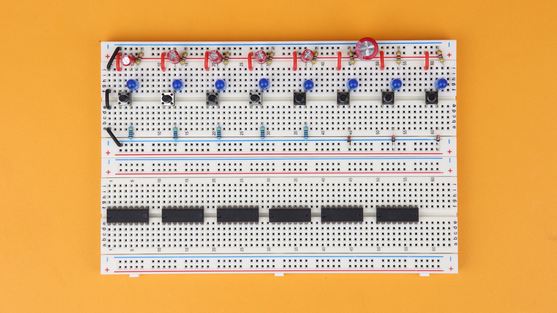
Now it's time to insert the integrated circuits. IC1 goes in row 1, IC2 in row 11, IC3 in row 21, then IC6 in row 31, IC4 in row 40, and IC5 in row 50. Make sure that all notches point to the left. Also make sure that IC6 (the CD4081 AND gate IC) is really plugged into the right position. It is the only IC we use that only has 14 pins (instead of the 16 pins of the CD4017 decimal counter ICs).
-
-
Step 11
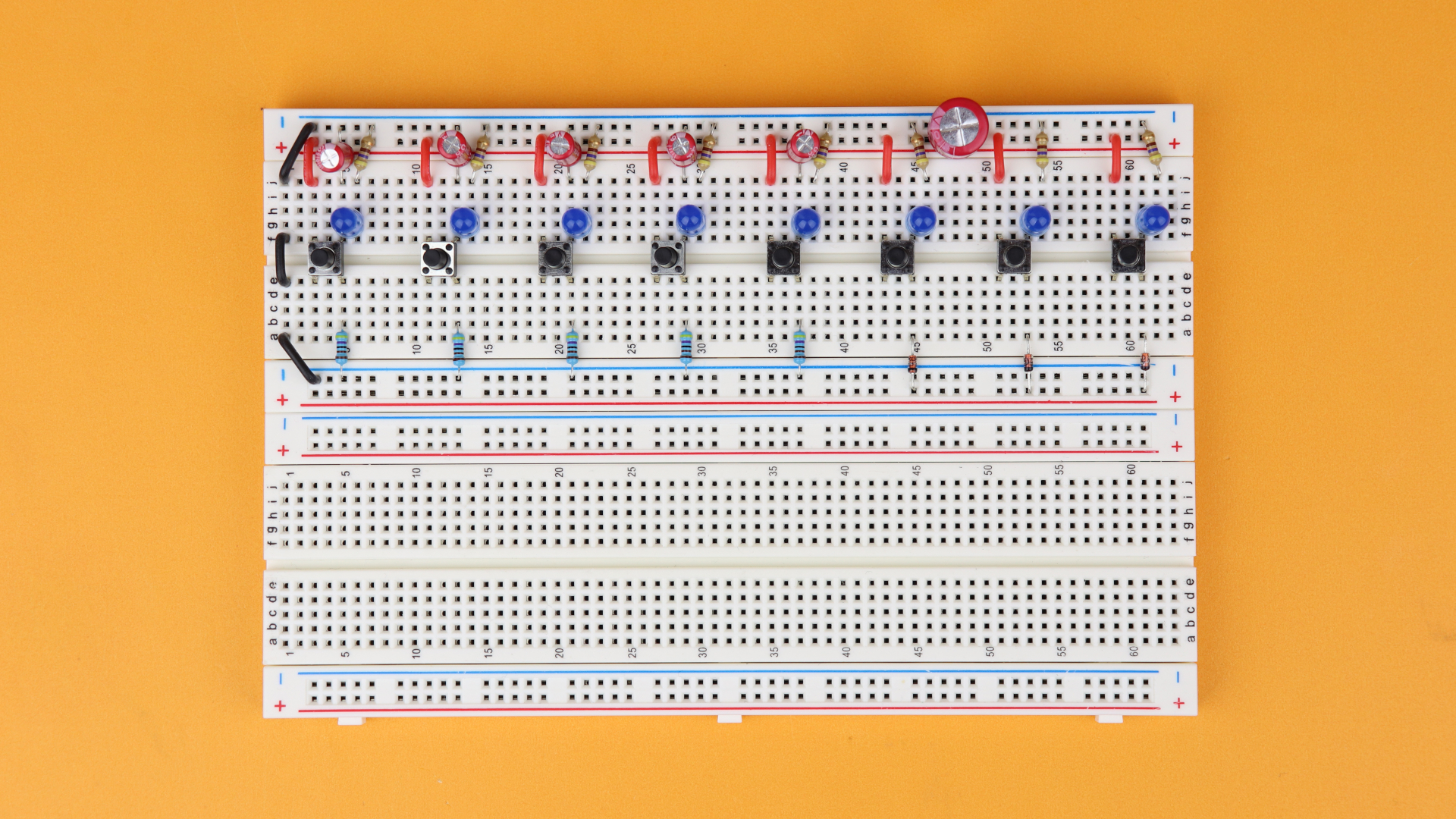
Connect the ICs to VDD on their top right pin (pin 16 for IC1–IC5, and pin 14 for IC6), and then connect them to ground on their bottom left pins (pin 8 for IC1–IC5 and pin 7 for IC6).
-
-
Step 12
Place the 100nF bypass capacitors C7–C12 between the power terminals of each integrated circuit. You can bend the leads as in the picture, but make sure the long lead faces towards the bottom of the breadboard, this way the wiring will be easier down the road. Also bend the leads carefully so that you don't accidentally short out any of the pins of the integrated circuits.
-
-
Step 13
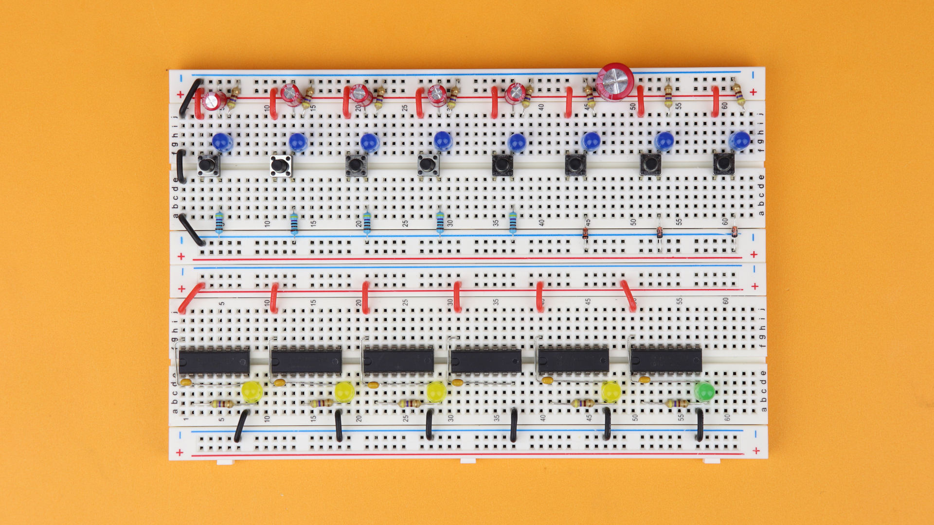
Next, insert the five status LEDs (LED9–LED13) and their 470Ω resistors R14–R18. The steps are very similar for each LED, but it is a bit hard to see in this single picture, so here we go for a detailed description:
Insert R14 between rows 2 and 9 and then LED9 between rows 8 and 9.
Insert R15 between rows 14 and 19 and then LED10 between rows 18 and 19.
Insert R16 between rows 22 and 29 and then LED11 between rows 28 and 29.
Insert R17 between rows 41 and 48 and then LED12 between rows 47 and 48.
Insert R18 between rows 51 and 58 and then LED13 between rows 57 and 58.All LED cathodes point to the left. I used a green LED for LED13, but the color choice is of course up to you :)
-
-
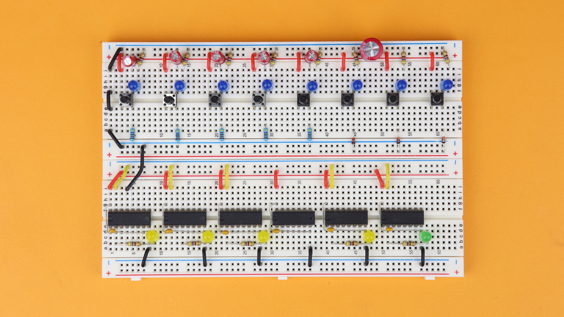
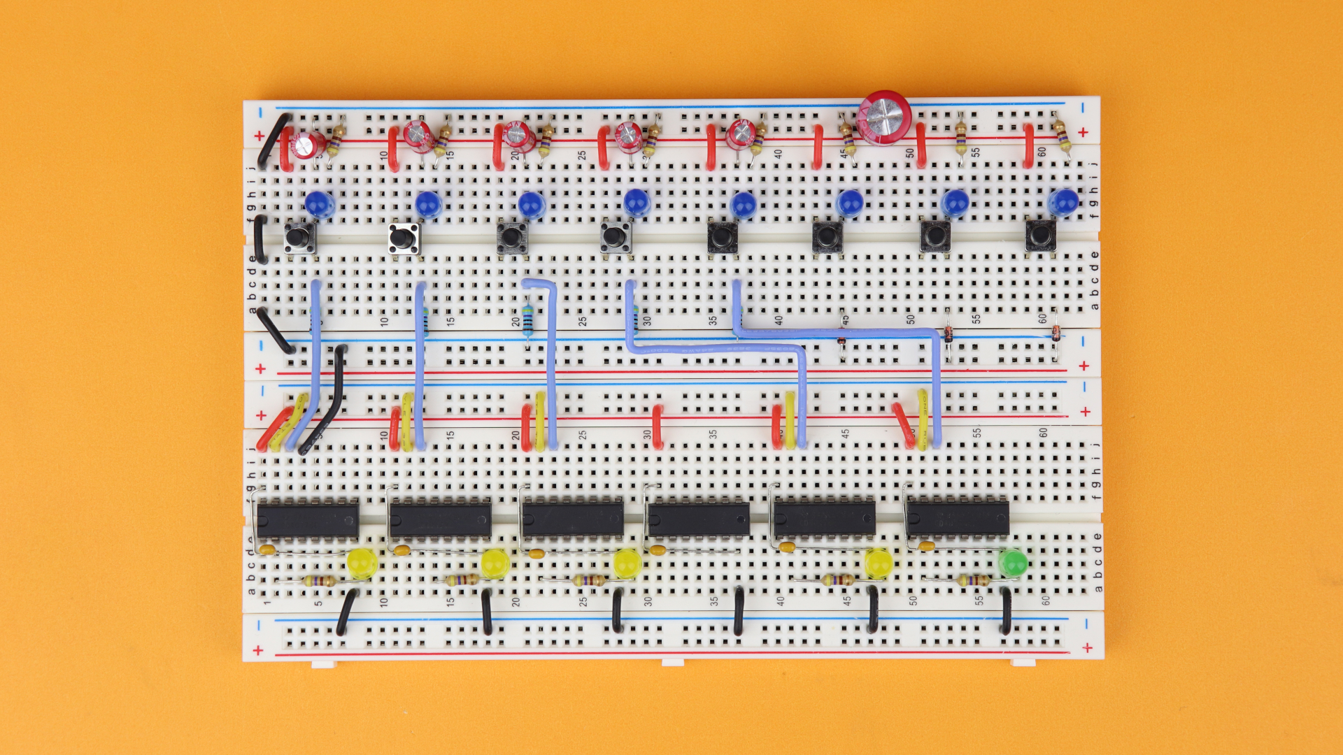
Step 14
Connect the clock inhibit input at pin 13 of IC1 to the ground rail (I used a black wire), and then connect all reset inputs at pin 15 of IC1–IC5 to the “reset signal” rail with the yellow wires (the upper ground rail of the lower breadboard).
-
-
Step 15
Now it's time to wire up the pushbuttons that are part of our combination. For the code A-BB-C-D-E you need to wire the switches as shown above, but you can of course use your own wiring if you want to change the code.
Connect the lower right terminals of SW1–SW5 to the clock inputs (pin 14) of IC1–IC5 with a blue wire.
-
-
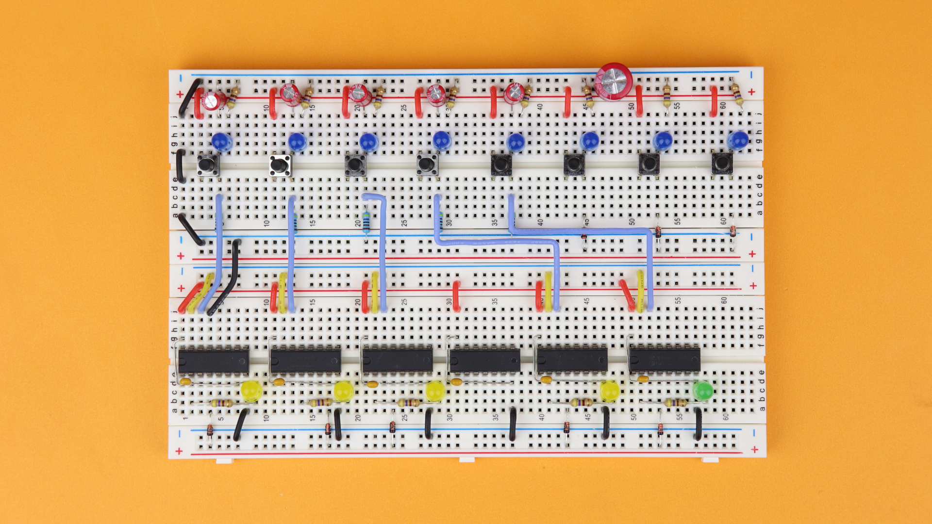
Step 16
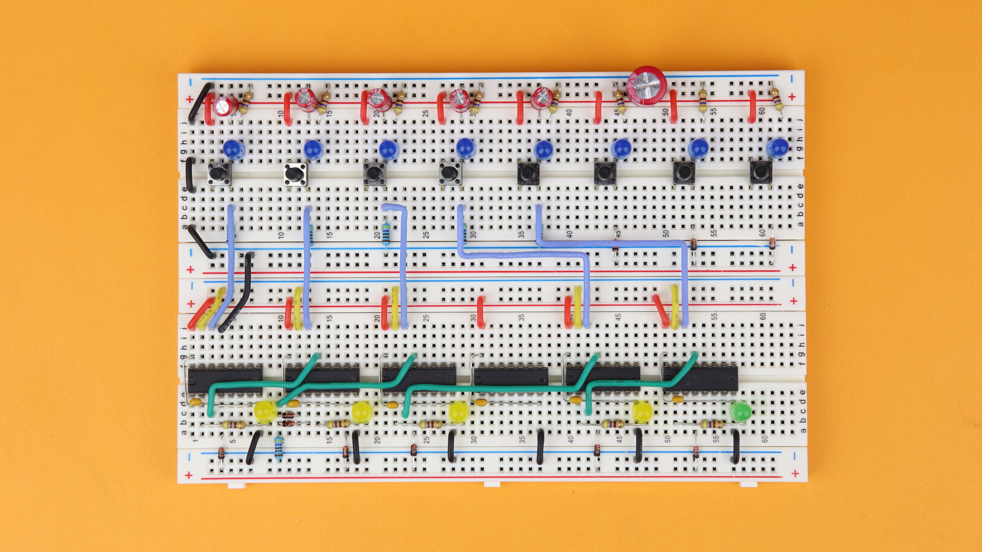
Now, insert the reset diodes D4–D8 from IC1–IC5 to the “reset trigger” rail (the lower VDD rail of the lower breadboard). Connect output Q2 (at pin 4) of IC1, IC3, IC4, and IC5 to the reset trigger rail, and output Q3 (at pin 7) of IC2 to the reset trigger rail. Important: Make sure that the diodes' cathodes (the black rings) are connected to the reset trigger rail facing down.
(I know, this sounds pedantic, but when I built this circuit the second time I had one diode the wrong way and I scratched my head for a day until I realized the silly mistake...)
-
-
Step 17
Connect output Q0 (pin 3) of IC1 to the clock inhibit input (pin 13) of IC2.
-
-
Step 18
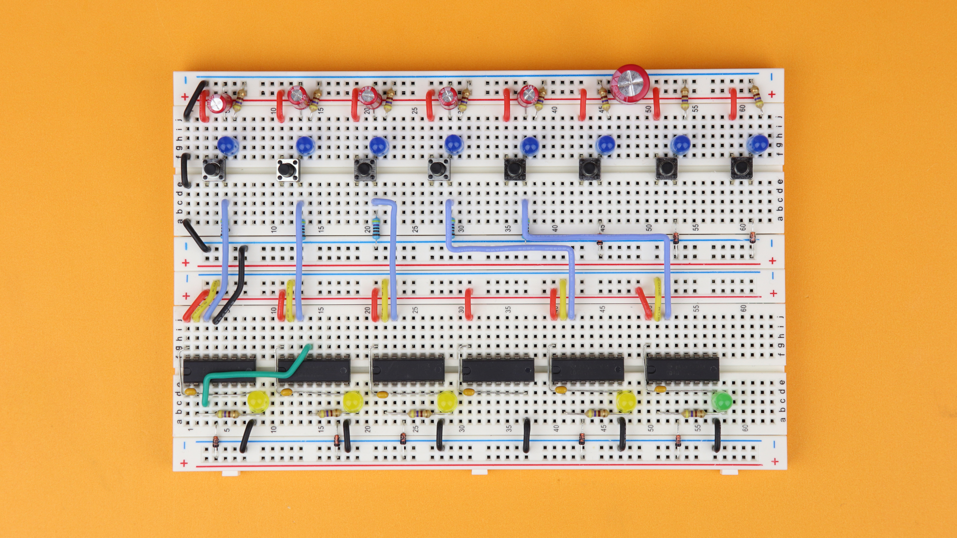
Insert diodes D9 and D10 from output Q0 (pin 3) and output Q1 (pin 2) of IC2 to row 10, with the diodes' cathodes facing to the left. Insert R15 between row 10 and the ground rail. And last, connect row 10 to the clock inhibit input (pin 13) of IC3.
-
-
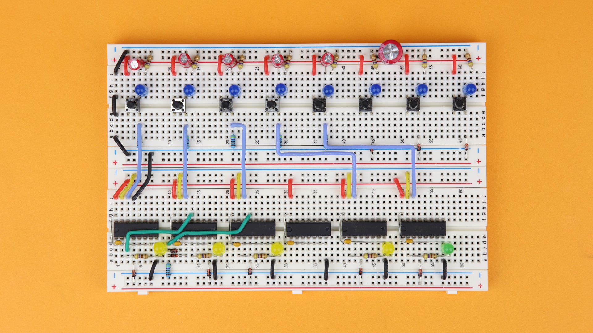
Step 19
Connect output Q0 (pin 3) of IC3 to the clock inhibit input (pin 13) of IC4, and then connect output Q0 (pin 3) of IC4 to the clock inhibit input (pin 13) of IC5.
-

-
Step 20
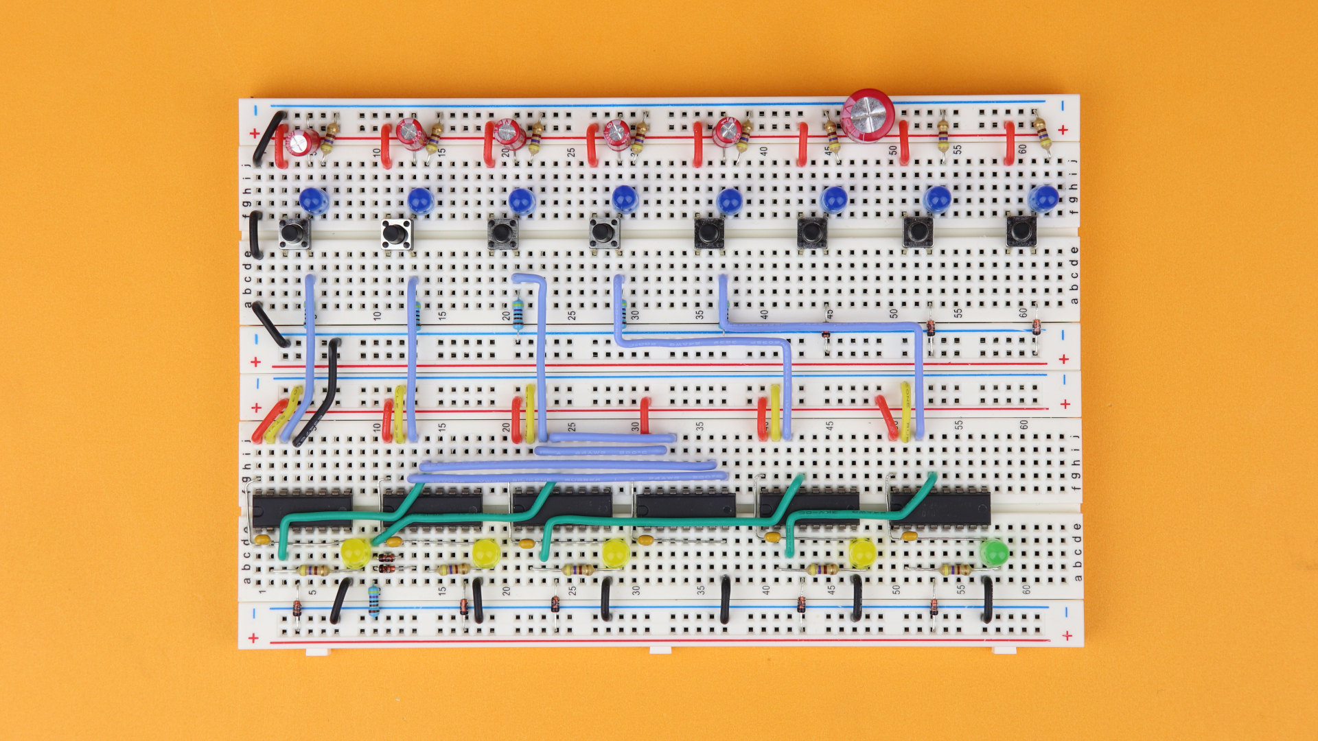
Now let's wire up the AND gates. This is the messiest part, so take some time and make sure all is connected properly. There are also pin numbers in the schematic, if you prefer. After these steps it gets better again, I promise :)
Alright, connect pin 9 of IC6 to pin 13 of IC2, and pin 8 of IC6 to pin 14 of IC2.
-
-
Step 21
Next, connect pin 12 of IC6 to pin 13 of IC3, and pin 13 of IC6 to pin 14 of IC3.
-
-
Step 22
Then, connect pin 1 of IC6 to pin 3 of IC3, and pin 2 of IC6 to pin 14 of IC4.
-

-
Step 23
And, finally, connect pin 6 of IC6 to pin 3 of IC4, and pin 5 of IC6 to pin 14 of IC5.
-
-
Step 24
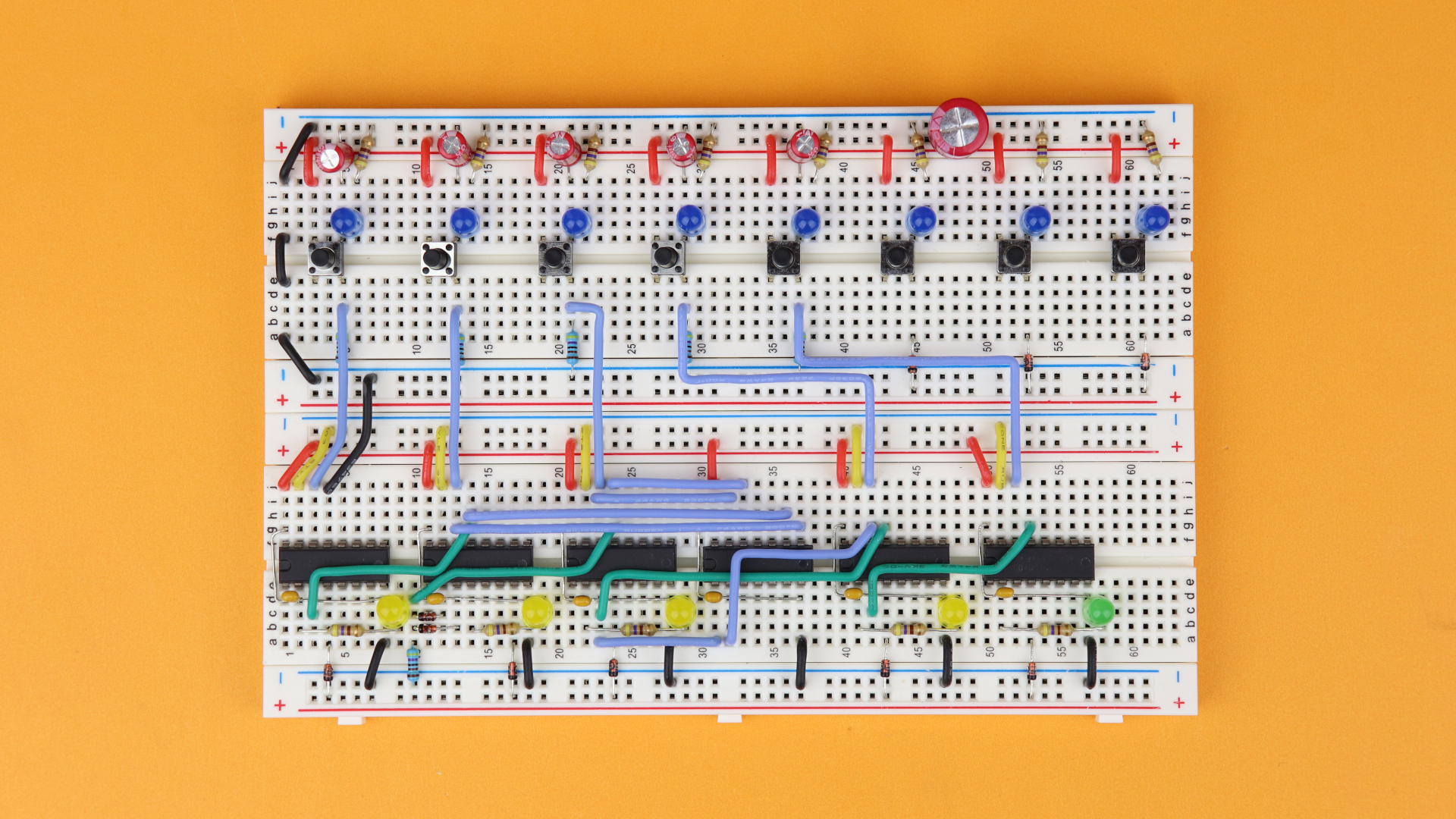
Now it's time to connect the outputs of our four AND gates to the “reset trigger” rail with the four diodes D11–D14.
Insert diodes from pins 3 and 4 of IC6 to the lower “reset trigger” rail, and two diodes from pins 10 and 11 of IC6 into the upper “reset trigger” rail. The cathodes (the black ring) are always connected to the reset rails.
-
-
Step 25
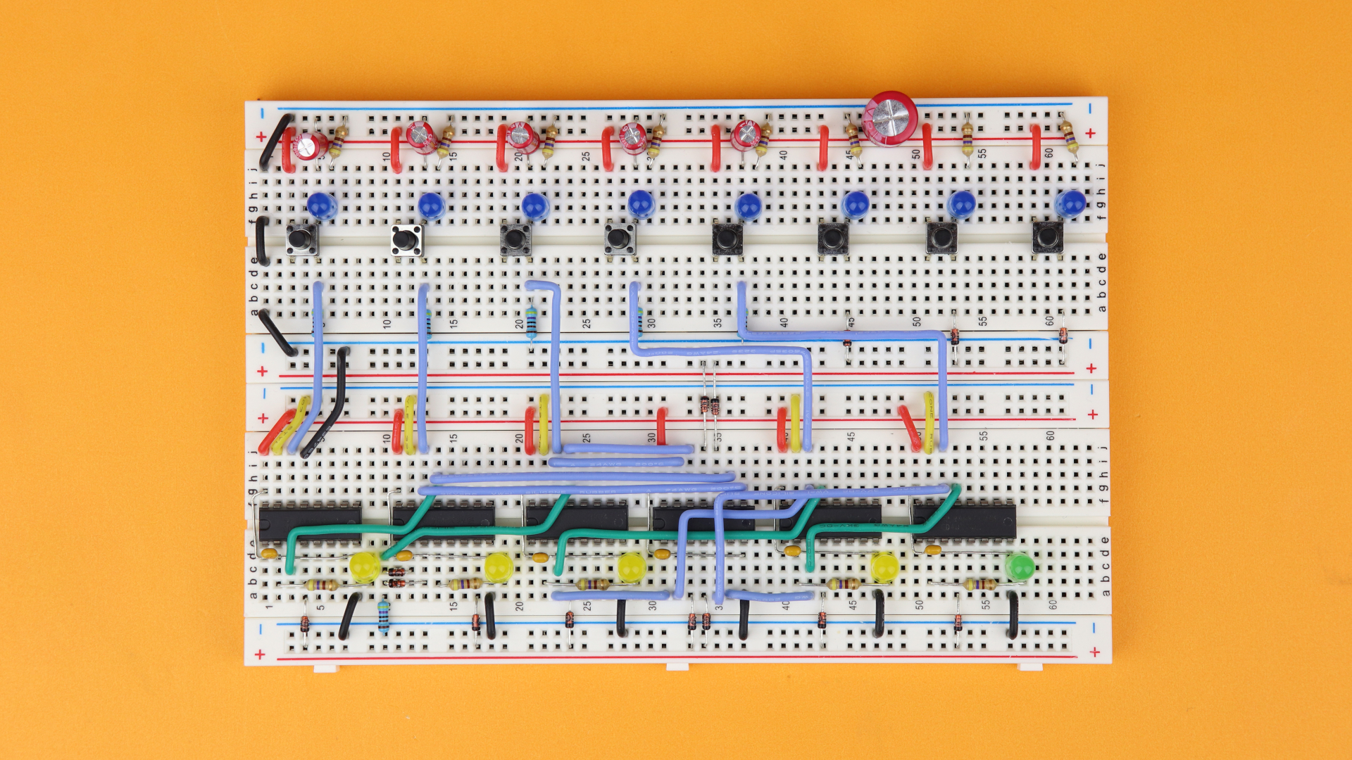
We are on the home stretch! Insert the NE555 timer (IC7) in row 60 with its notch facing to the left. Connect pin 8 to VDD, pin 1 to ground, and insert the 100nF bypass capacitor C13 in between. Also connect the 10nF stabilizing capacitor C14 between pin 5 and the ground rail. Make sure that its lead does not touch the diode's cathode, you can bend it out of the way a bit more than in the picture, just to be safe.
-
-
Step 26
Connect pins 2 and 7, and then pins 6 and 7. Insert R20 between pin 7 and VDD, and R21 between pins 3 and 4.
-
-
Step 27
The 22μF timing capacitor C15 goes between pins 1 and 2, with its negative terminal (the one with the big minus sign) connected to pin 1.
-
-
Step 28
Next, connect the NE555's /RESET input at pin 4 to the “reset trigger” rails with yellow wires. Remember: we are using the lower VDD power rail of the upper breadboard, as well as the lower VDD power rail of the lower breadboard, as “reset trigger” rails to save us some wiring.
-
-
Step 29
And, finally, connect the NE555's output at pin 3 to the “reset signal” rail (the upper ground rail of the lower breadboard).
-
-
Step 30
Now it's time for the reset LED. Insert the 470Ω resistor R22 between the “reset signal” rail and row 48 on the upper side of the lower breadboard, and insert LED14 between rows 48 and 49 with its cathode facing to the right. Then use two black wires to cross over from row 49 on the upper part of the breadboard to the lower part, and then further down into the ground rail.
-
-
Step 31
Now we have to make sure that all power rails are connected to each other. Connect the upper VDD rail on the upper breadboard to the upper VDD rail on the lower breadboard, and then connect the lower ground rail on the upper breadboard to the lower ground rail on the lower breadboard. Yeah, I know, but it sounds worse than it is :)
-
-
Step 32
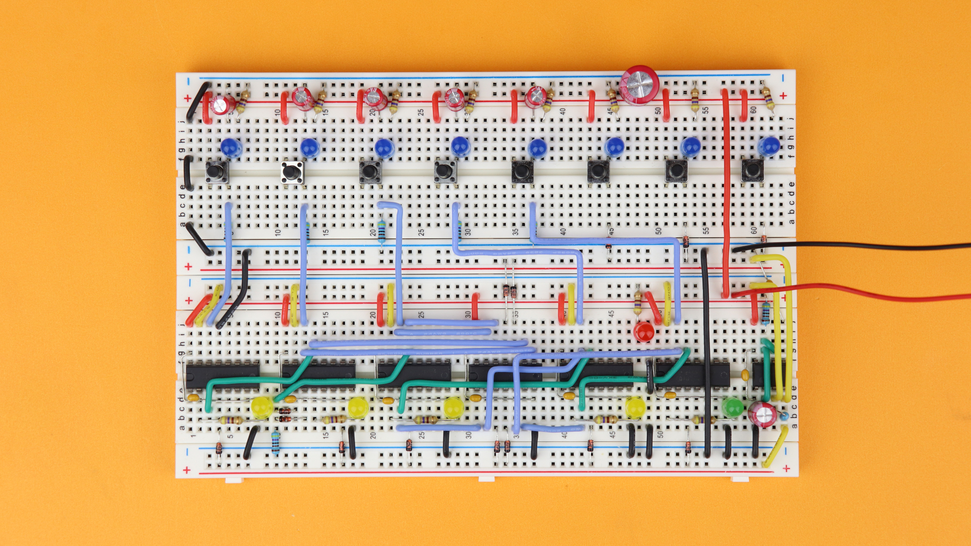
And, finally, you can connect the 9V battery clip. The positive terminal (the red wire) goes into the VDD power rail, and its negative terminal (the black wire) is connected to the ground rail.
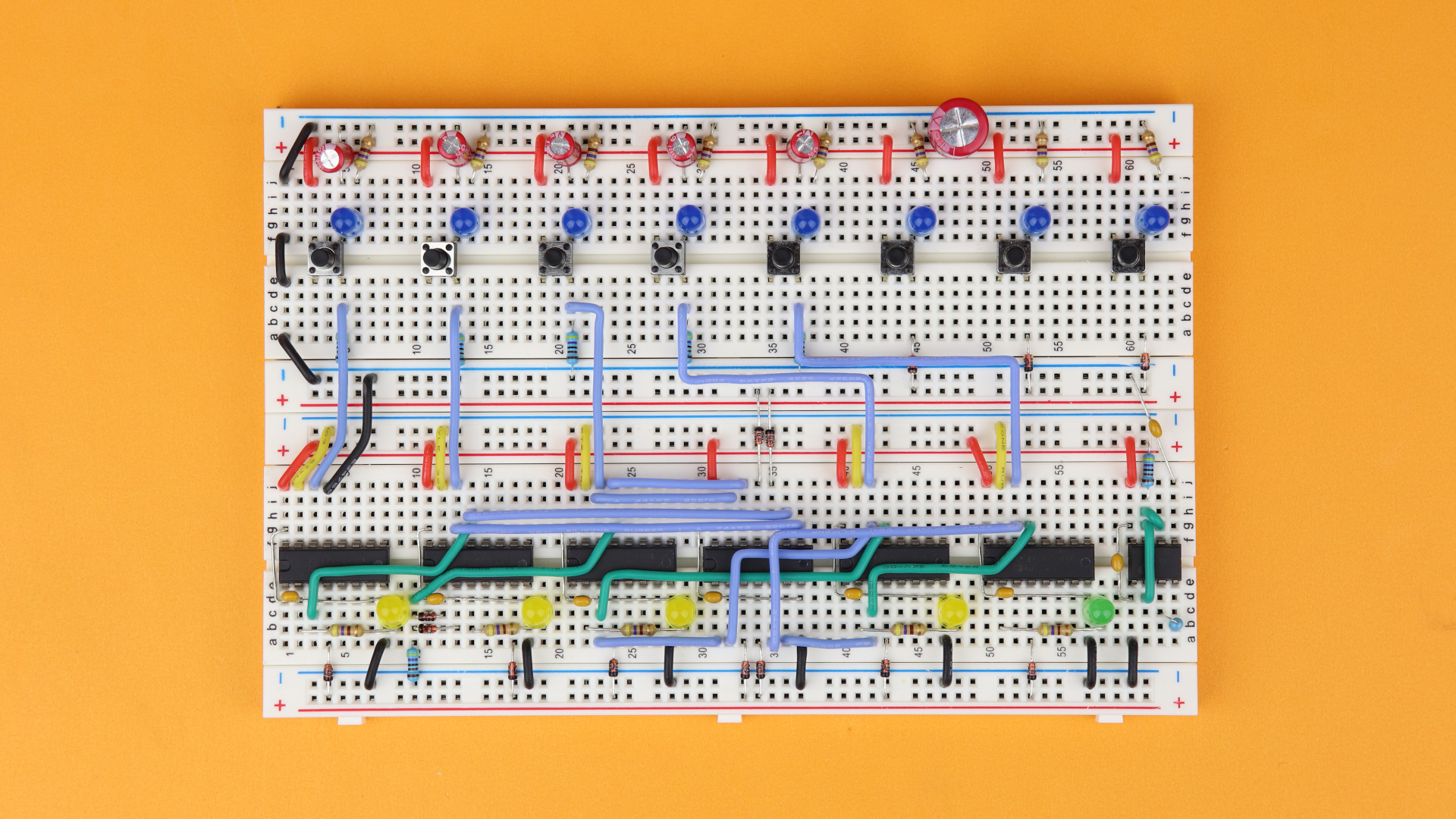
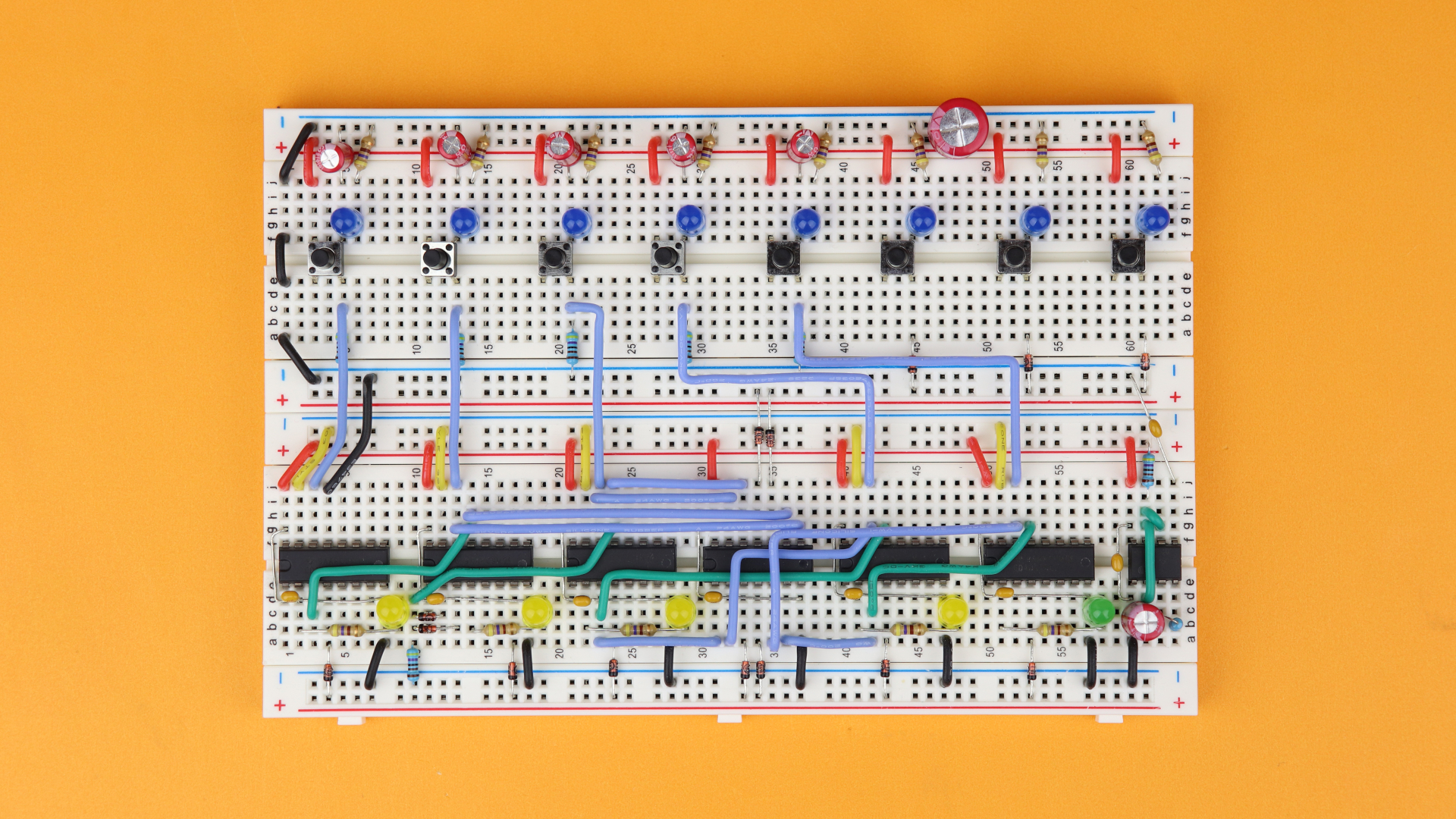
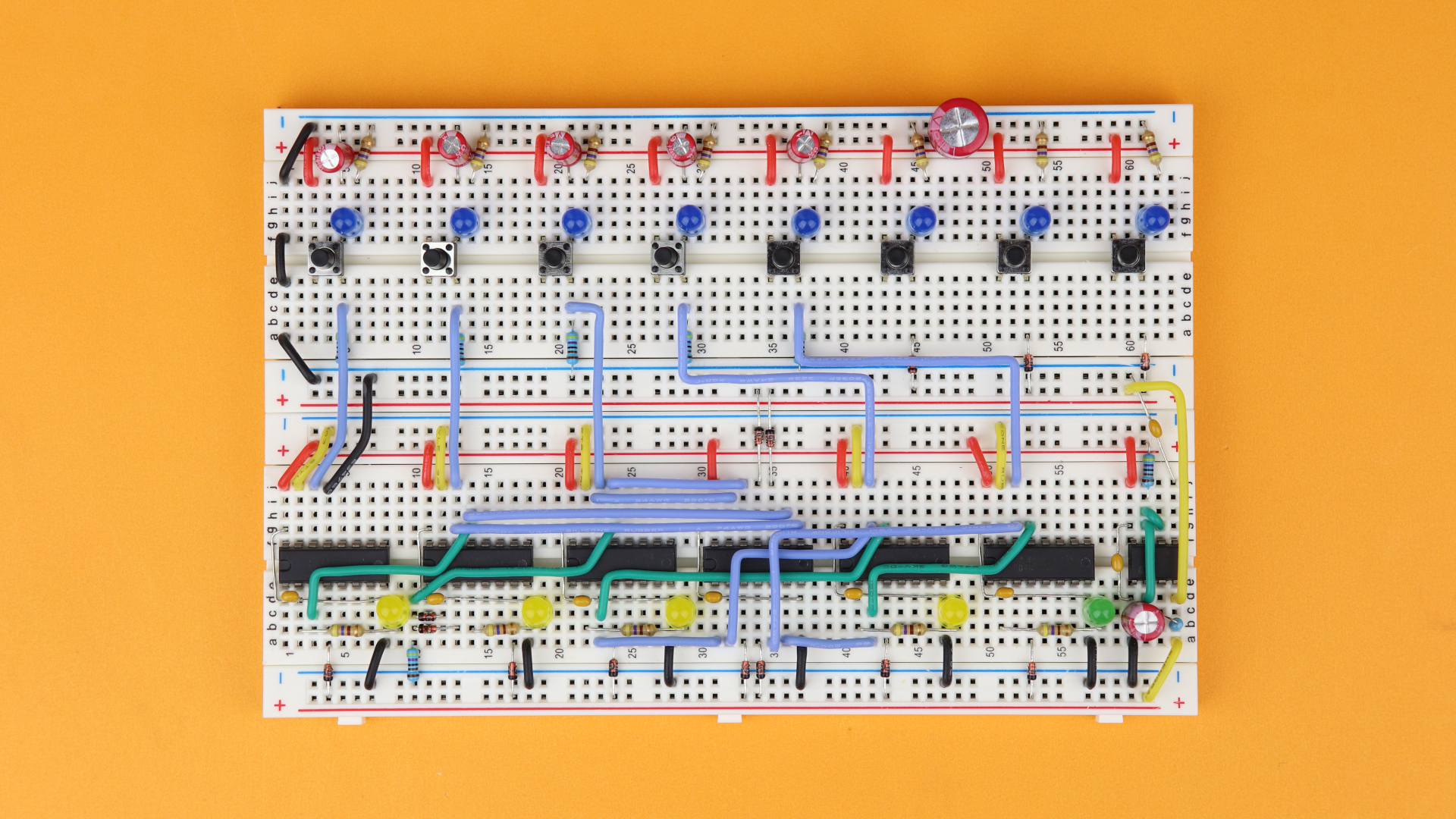
And congratulations, you are done! Whenever you plug in the 9V battery, the red LED should flash very briefly (70ms). Then you can enter the code A-BB-C-D-E, and it should look like this:
And now you can play around! Change to code by changing how you connect A, B, C, D, and E to the circuit, or insert more diodes to change the code from A-BB-C-D-E to A-BBB-CC-D-E, and so on :)
YouTube video
I covered this entire project in a dedicated YouTube video:
Final thoughts
And that wraps it up! But as always there are some comments and thoughts that came to me while working on this project, and I would like to share them with you here.
- The main problem with this schematic is that it does not support all codes: codes like A-B-A-C-D are impossible. I am not sure if there is a simple workaround, or if it would require a ton of more components. If you find a clever way, let me know!
- So why not just use a microcontroller? That's true, with a microcontroller you could built this circuit in a fraction of the time in a fraction of the space with a lot more functionality. The goal of this project was to use a commonly available component (the CD4017 decimal counter) and use it to build something unusual. But if space or efficiency is your primary concern, then by all means: use a microcontroller :)
- The placement of the debounce capacitors C1–C5 and pulldown resistors R9–13 on the breadboard is not ideal. They are placed next to the pushbuttons but should, logically, be placed next to the counter. This way it would be easier to change the code later on. But the constraints of the breadboard made it difficult for me to find a place for the debounce capacitors and pulldown resistors close do their counters.
So when you build this circuit yourself and want to use a different code from A-BB-C-D-E, then keep in mind that the debounce capacitors have to move around as well.
This reminds me of the analogy that a schematic is like a subway map, whereas the breadboard is like the actual subway system underground. They are topologically equivalent, but the schematic is always the abstraction, and the circuit is the real-life implementation :)
There are also several addons/improvements that could be made to this circuit:
- Can you add a wrong code attempt counter? For that you could use either another CD4017 or the CD4026 7-segment counter. Make sure to @ me on Twitter if you build anything like that, I would love to see a photo or video!
- It would also be cool to have something more dramatic happen if you unlock the code lock (except for the green LED turning on). You could connect it to external circuits with a driver to turn on your coffee machine, or something else. Maybe I will make a separate video about that some time!
- As I said before: In a secure code lock, the intermediate indicator LEDs LED9–LED12 are a very bad idea because they give away the code. Unless you add many many keys, then it can become a nice game of memory! Here I just included them to make the circuit visually more appealing and intuitive :)
And the last thought is this: how many combinations does this code lock actually have? ... So we see: Adding more keys makes it more secure!
I really hope you enjoyed this project, and thank you for your time. Let me know what else you want to learn, and I will see you next time! Thanks for reading!