Three wires to rule them all: CD4094 & CD4021 shift register tutorial
December 17, 2022 • tutorial
What do you do when your microcontroller does not have enough pins? In this tutorial we will learn how to use shift registers to control LEDs and to read out pushbuttons, all with just three wires! In six steps, we will learn all about the CD4094 output-type shift register, the CD4021 input-type shift register, and how to use them with a PIC microcontroller. And in the end we will pit it all to use with an SNES game controller, which—you guessed it—also uses shift registers on the inside.
What you need
In this tutorial we will use quite a lot of components:
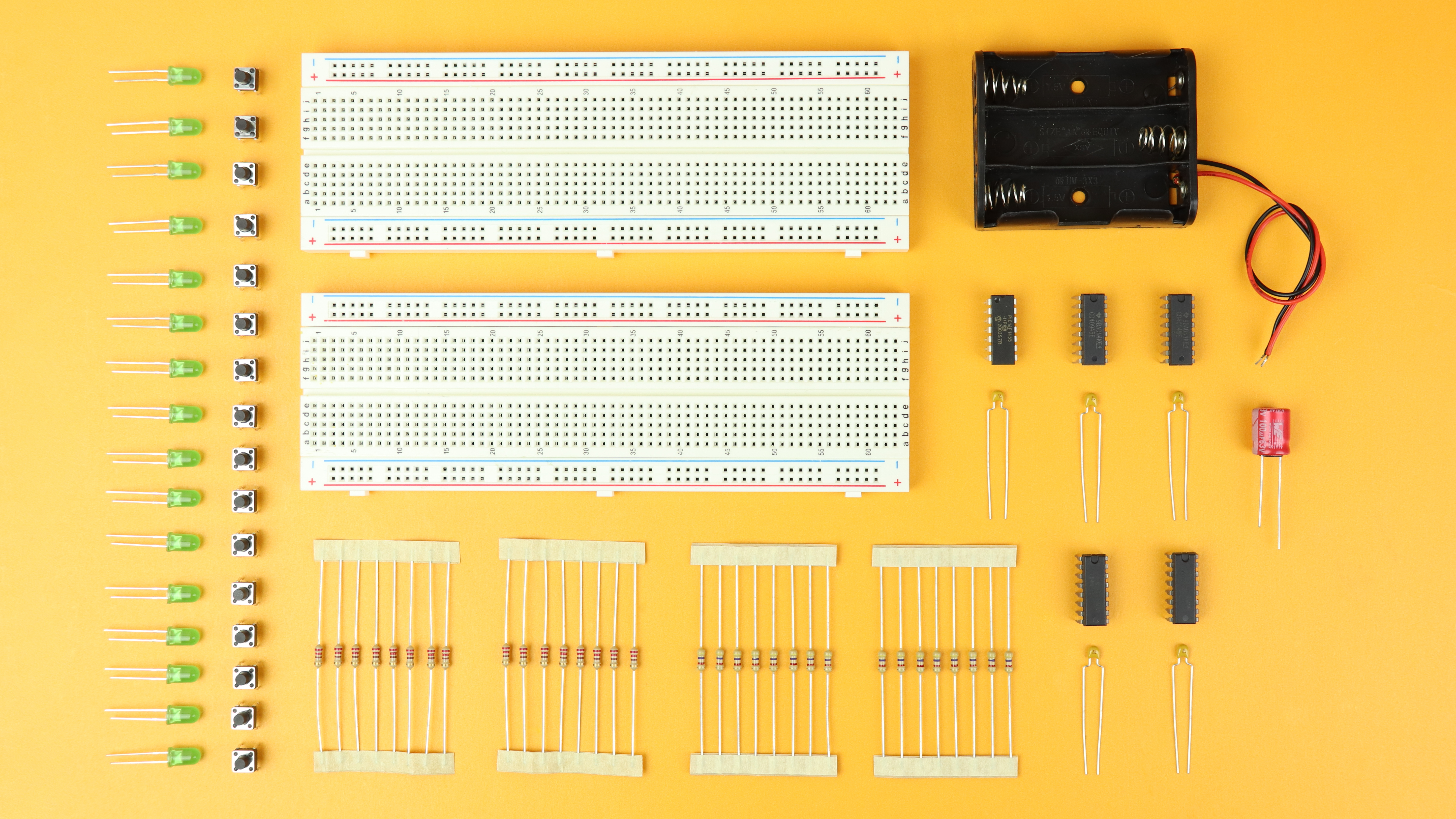
As usual, you can find a detailed list in the components box. The main for today's tutorial are:
- The CD4094 output-type shift register. We will use this shift register to control simple 5mm LEDs.
- The CD4021 input-type shift register, which we will use to read out the status of pushbuttons.
- A PIC16F1455 microcontroller. We could use any other PIC microcontroller, too, and the relevant code to interact with the shift registers works exactly the same on any microcontroller.
- Other than that, we just need some LEDs, resistors, capacitors, pushbuttons, breadboards, and wires :)
So let's get started with our main idea for today!
Main idea
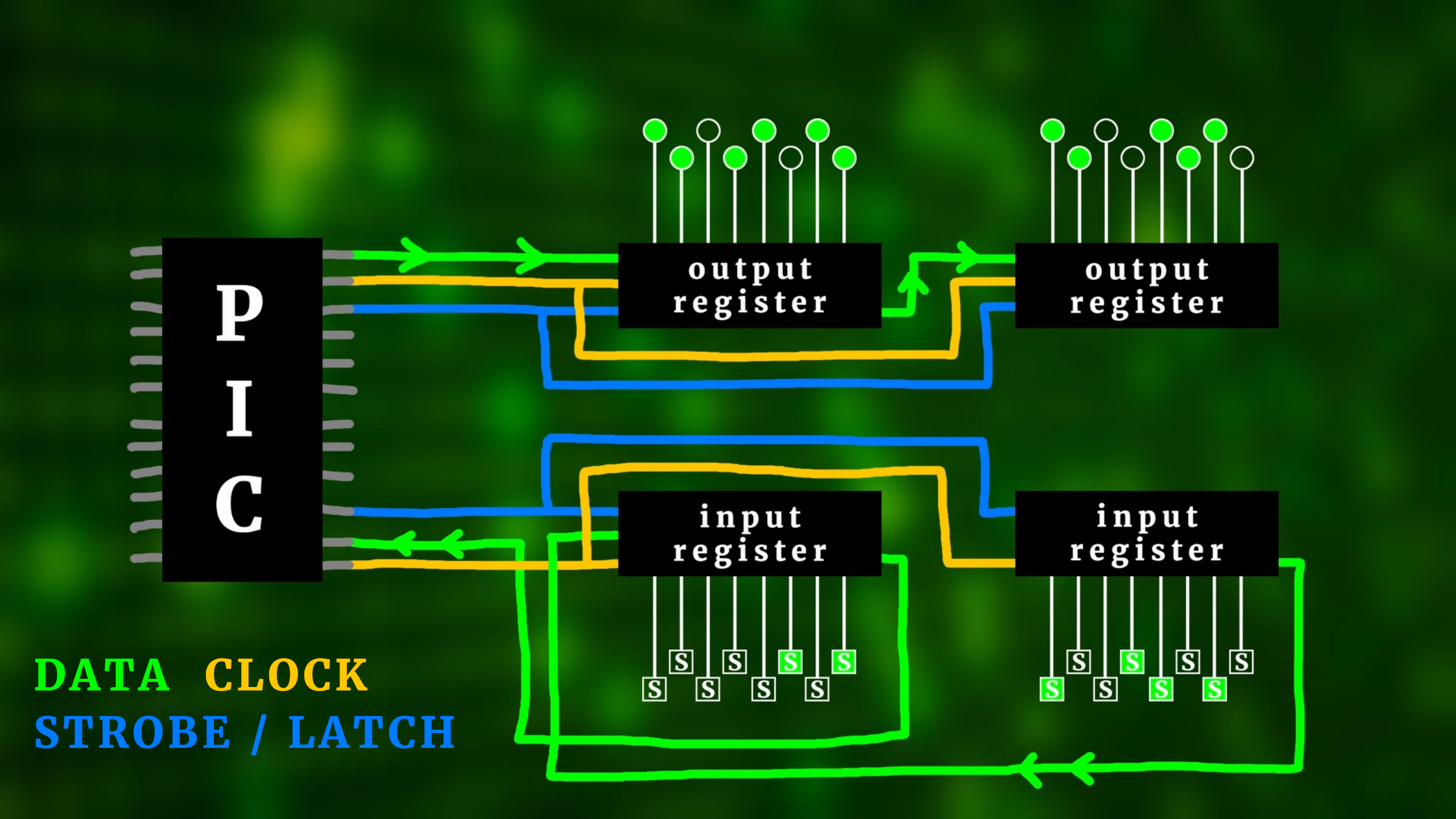
So here's the main idea of our circuit today. On the left is our PIC microcontroller with only a few pins.
The LEDs that we want to control are connected to an output-type shift register, and the pushbuttons we want to read out are connected to an input type shift register. At this point we don't save any pins or wire at all, each LED and each button needs to be connected separately to its register.
But a shift register only needs three wires to talk to our microcontroller, and those are the precious connections we want to keep as few as possible. So, with three wires, you can control eight LED's, and with another three, you can read out eight buttons as well.
But it's even better than that! You can chain shift registers of the same type behind each other, so that in theory it's possible to control an unlimited amount of LEDs, and read out an unlimited amount of buttons. This works because shift registers turn so-called parallel data (which is a snapshot of the state of all LEDs, or the state of all buttons, all at one common time) into so-called serial data (which is a sequence of individual bits, one after the other, for each LED and pushbutton).
So now let's learn in detail how these two types of shift registers work on the inside!
CD4094 & CD4021: how do they work?
Instead of going through how these registers work on a fundamental level with flip flops, I want to give a simplified mechanical explanation instead that will do it justice for our purposes today. So let's go!
(There is a YouTube video for this entire tutorial! Make sure to check it out, too; especially the next part is more difficult to explain with words, and moving images really help to make the idea of shift registers easier to grasp.)
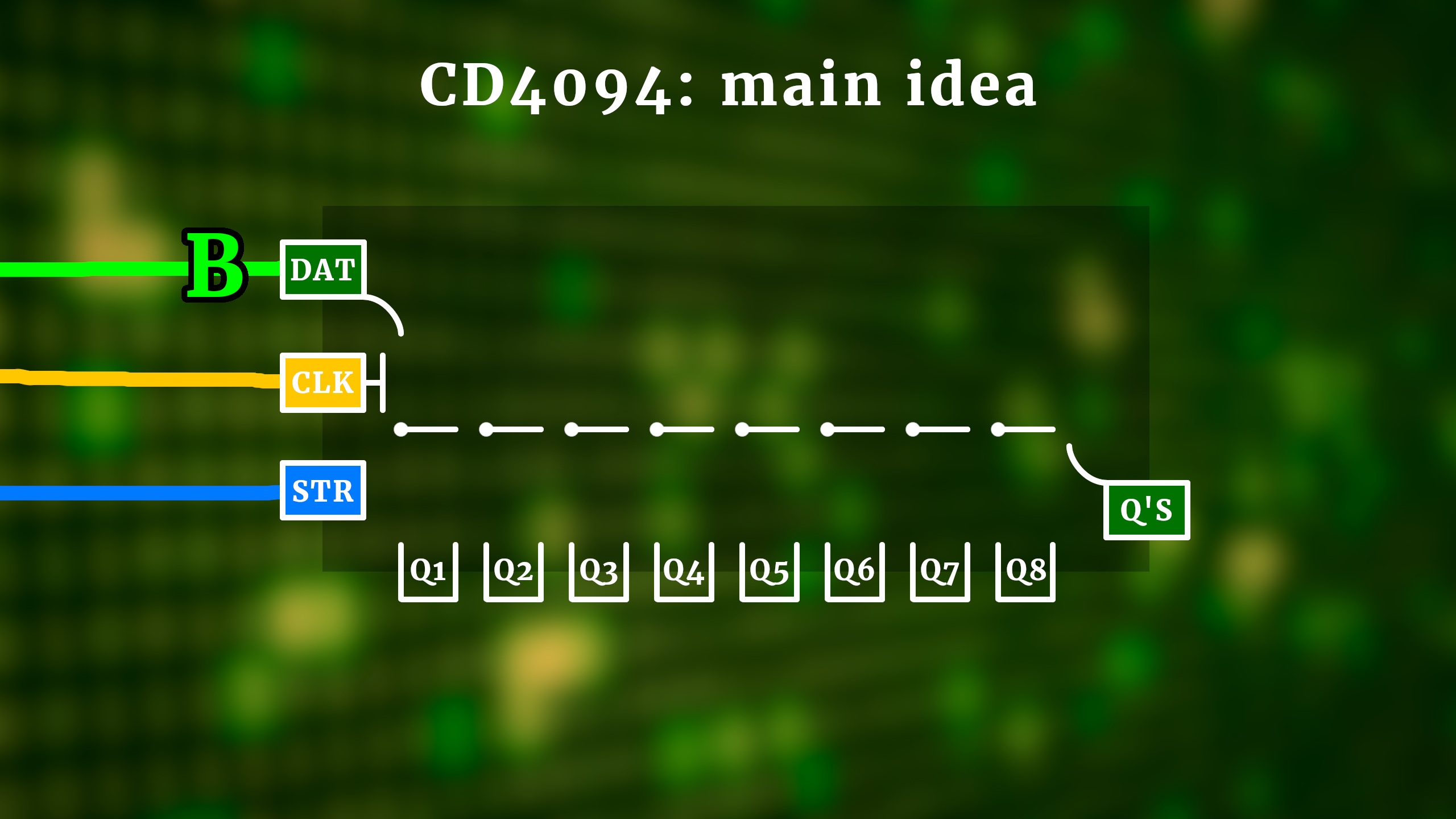
Let's start with the CD4094 output type shift register:

It has three inputs (DATA, CLOCK, and STROBE) and eight outputs Q1-Q8 as well as an extra output called Q'S. Because it can hold eight bits, this is an eight-bit shift register.
In our case, we will connect the DATA, CLOCK, and STROBE inputs to our microcontroller. That's our three wires we need for this operation.
Now how do we get data into this register with these three wires? Let's say we want to get a bit B into it. First, we have to make sure that CLOCK and STROBE are low. Then we can apply this bit at the DATA input:
Keeping STROBE low, we can now pulse CLOCK from 0 to 1 and back to 0 again, and after that we are here:
if we now pulse CLOCK again, it kind of acts like a piston and pushes the bit one place further:
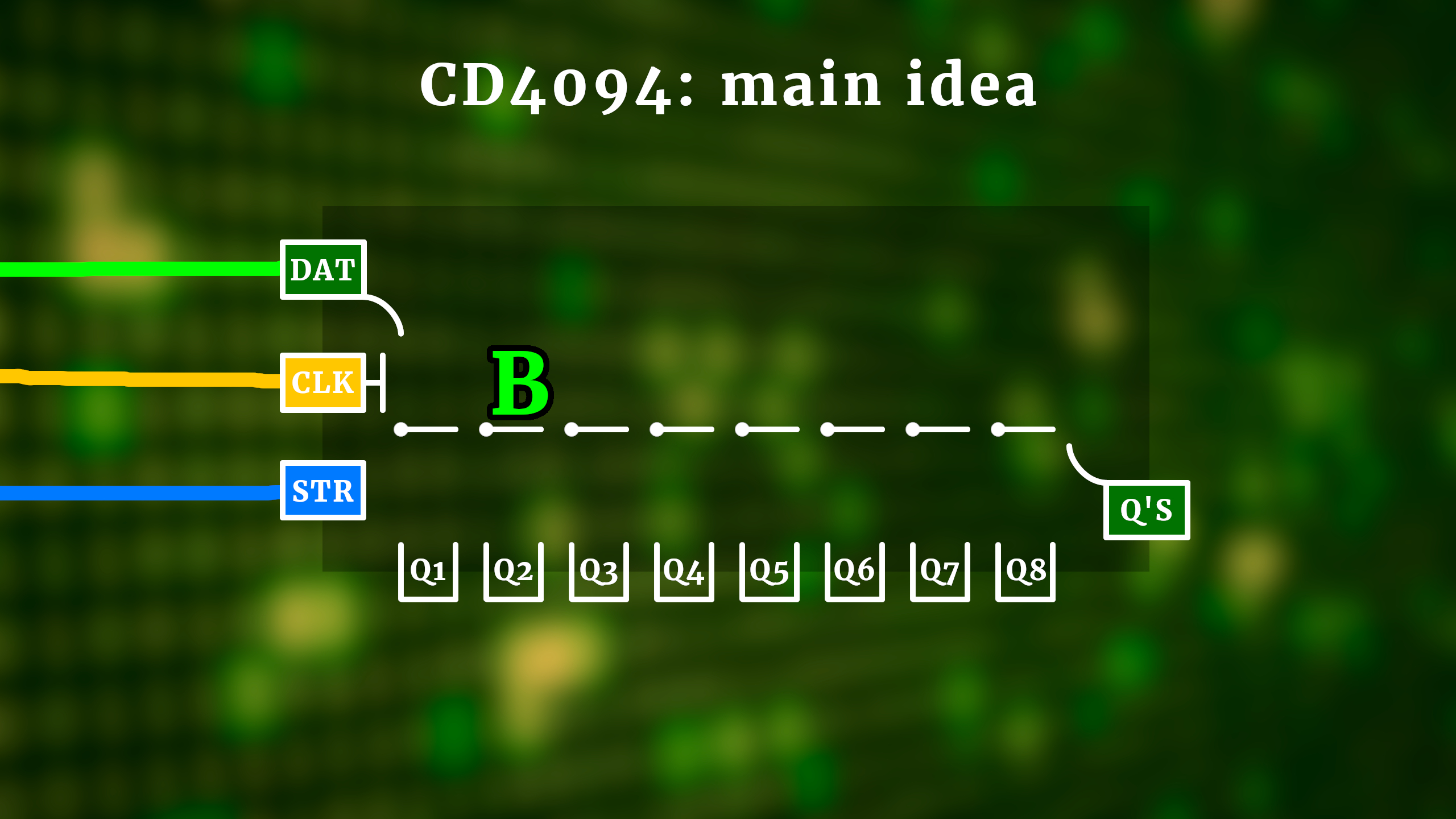
And of course now whatever signal is on the DATA input will fall into the register, too (watch the YouTube video for a better visualzation). But now we can also apply a pulse to STROBE. Then, the current status gets duplicated to the outputs of the CD4094 like that:
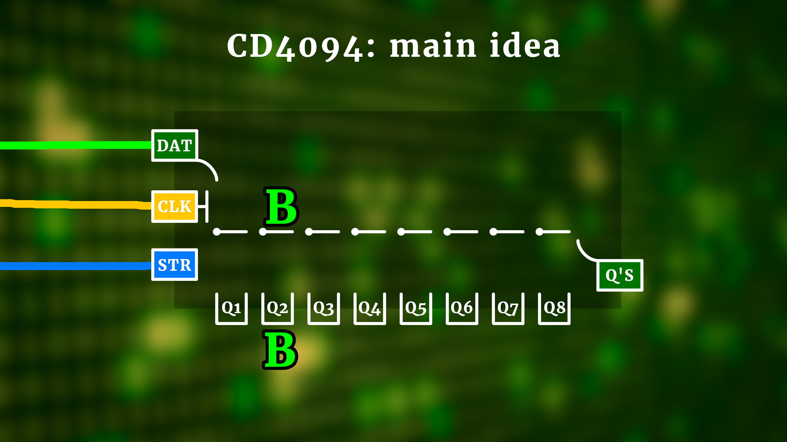
The idea is to think of these little platforms that the bits are moving on as trapdoors, and pulsing STROBE opens those trapdoors. Anyway, you can imagine if you keep pulsing CLOCK, eventually the bit will arrive at the end of the register:
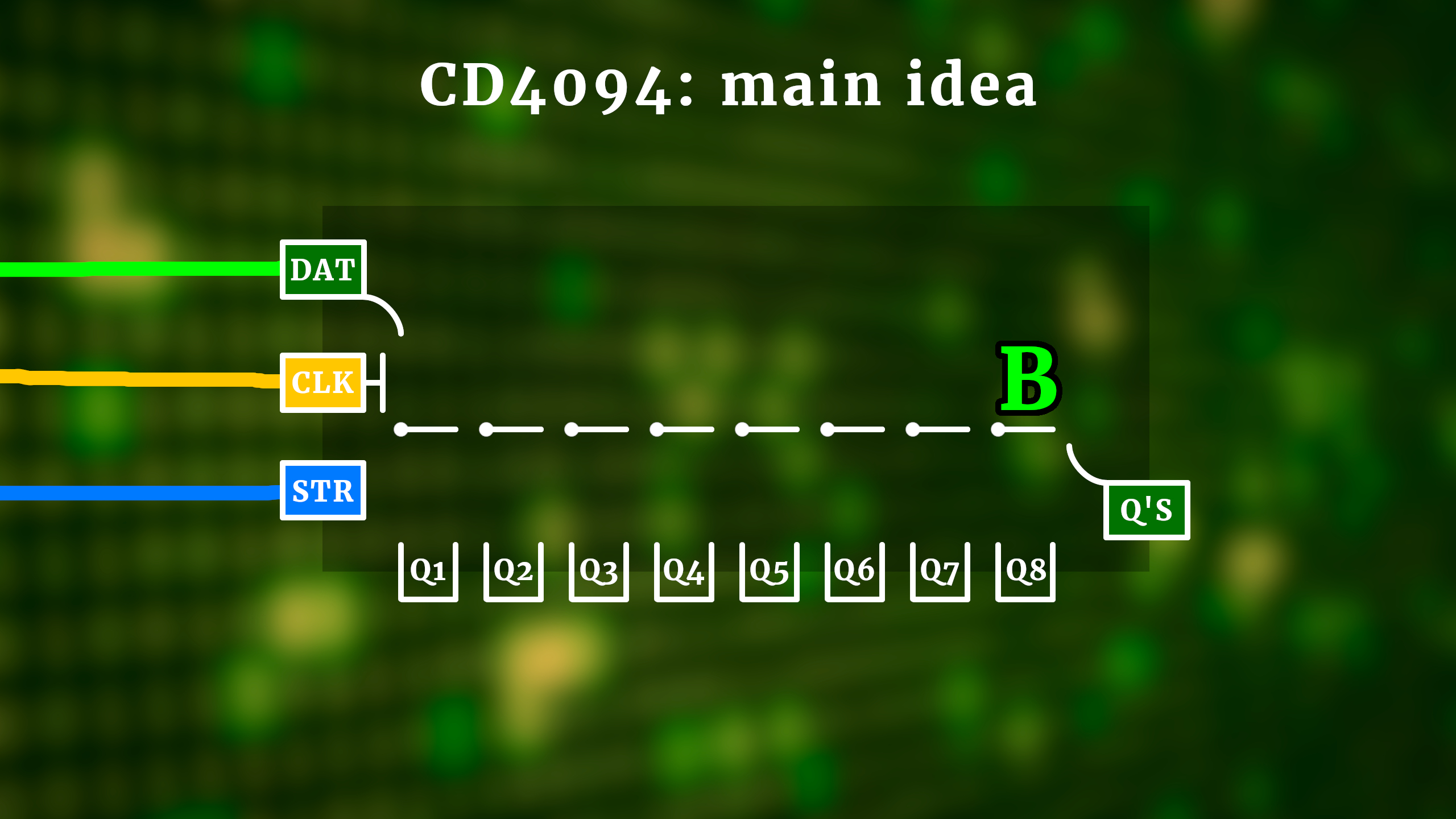
If you now pulse CLOCK one more time, the bit will fall out, and appear on the Q'S output:

And you can imagine that now it's a good idea to connect the DATA input of a new register to the Q'S output of this one, so the data doesn't get lost, but merely gets transported further down the chain. Here is how that could look like:

The nice thing is that CLOCK and STROBE are connected in parallel, and the DATA input is connected from the microcontroller only to the first register. So you see: three wires is enough to control as many LEDs as you like.
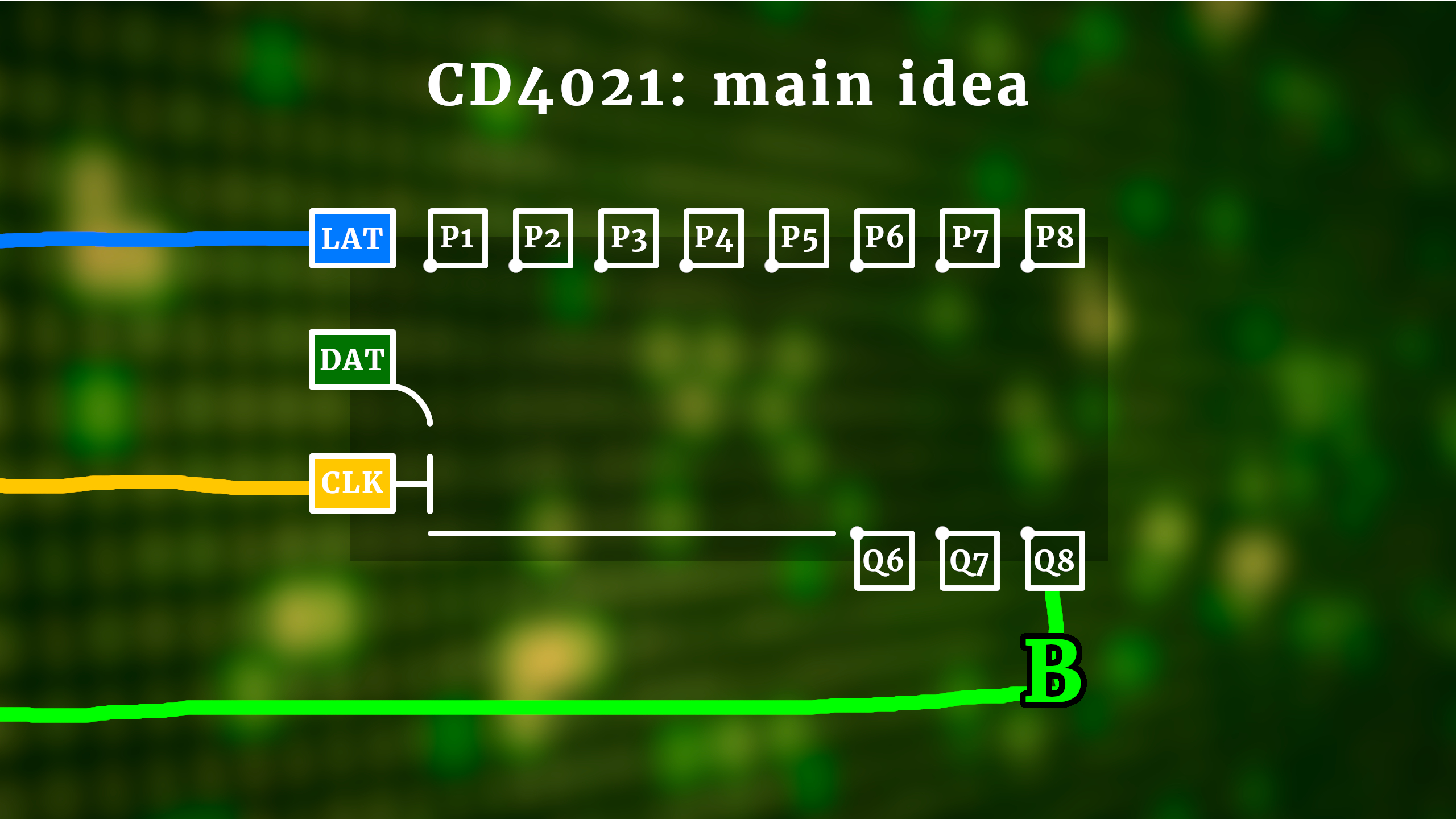
Now how about the CD4021 input-type shift register?

It has eight inputs, called P1-P8, which is where we will connect our pushbuttons. (It also has another DATA input, which we will talk about later.) Other than that, it has a CLOCK and LATCH input as well. On the output side there are three outputs, called Q6, Q7, and Q8.
In our case, we will connect the CLOCK and LATCH inputs to our microcontroller, as well as the Q8 output to read out the data. That's our three wires we need for this operation.
Now how can we read out the status of each input P1-P8 with these three wires? Imagine that we are interested what happens at input P5:

We first need to pulse the LATCH pin, which transfers the status of all inputs into the register (of course, all the bits from each input fall into the CD4021 when pulsing LATCH, I am only showing the bit at P5 to keep things easier to follow):

Then (and that part is similar to the CD4094) we need to pluse CLOCK, and for each pulse, the bit moves further down the register.
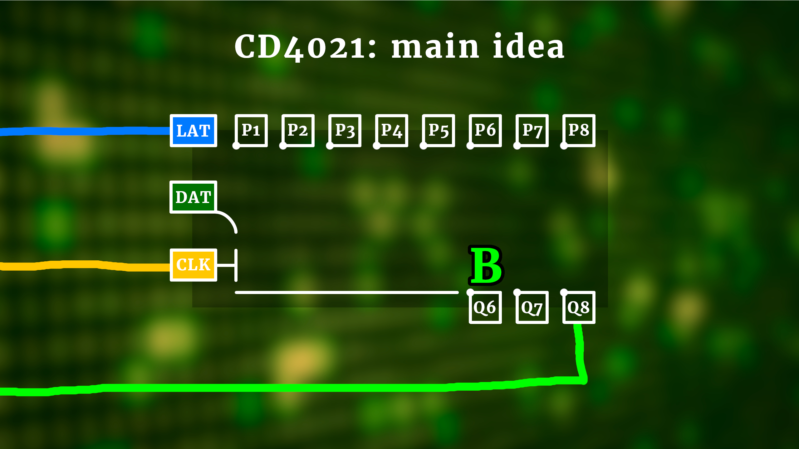
As soon as it is above Q6, Q7, or Q8, its status gets duplicated to these outputs; in other words, the three outputs Q6, Q7, and Q8 always show what is going on in the last three places inside the reguster. Eventually, after two more CLOCK pulses, our bit reaches Q8.
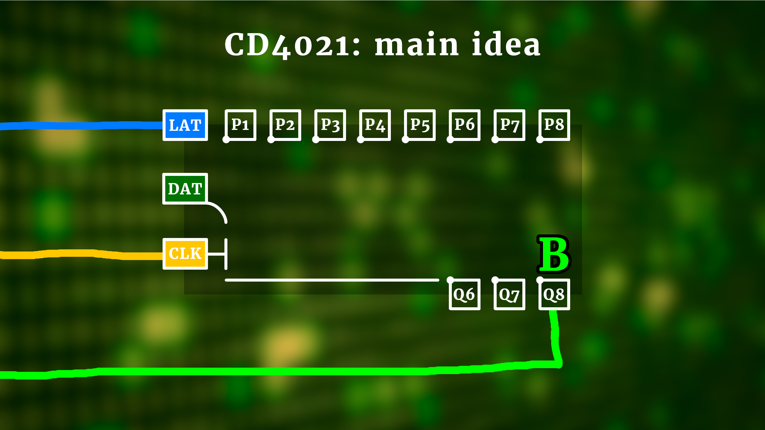
And then it gets duplicated to the Q8 output, where our microcontroller can then read it out.
And that's really the main idea. Now, how do you chain these registers together? For that we need the DATA input. When LATCH is low, and we pulse CLOCK, whatever is on the DATA input gets passed along the chain. This way we can construct a chain of several CD4021 registers, simply by connecting the Q8 output of the next CD4021 in line (the one we just added) to the DATA input of our original CD4021:

This doesn't look as clean as in the CD4094 example, but that is just because I chose the bits to travel from left to right in my somewhat random and arbitrary visualization. So even though it looks a bit messy, it is exactly the same idea as in the CD4094 case: data doesn't get lost, it just moves on to the next register in the chain.
But now, after all that talking, let's put it to the test and try to make these registers work in some real-life examples.
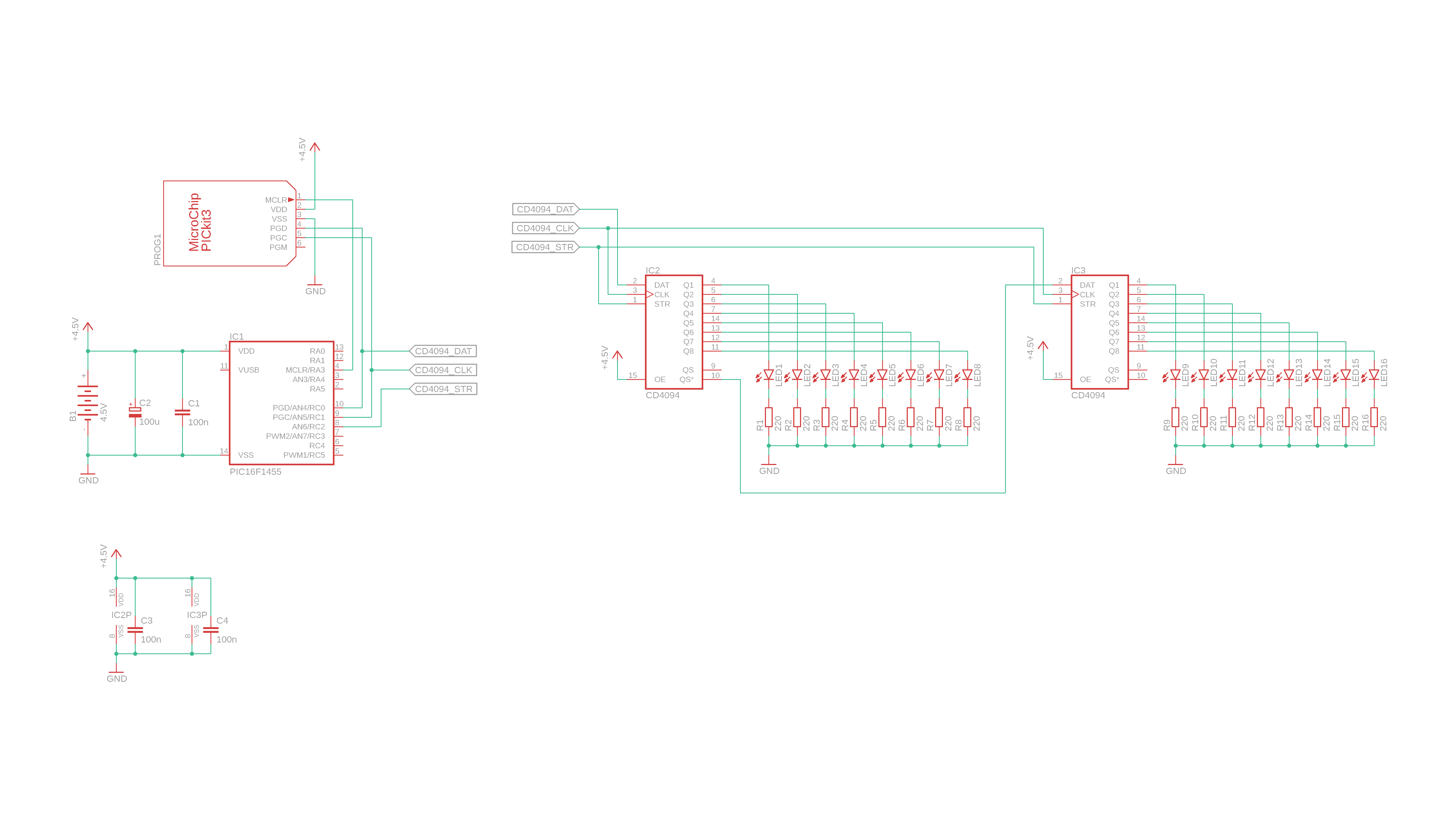
Setting up the PIC16F1455
Now that we understand those basics, let us try to send out some data to the CD4094, and receive some data from the CD4021. To do that, we first build this simple circuit here:

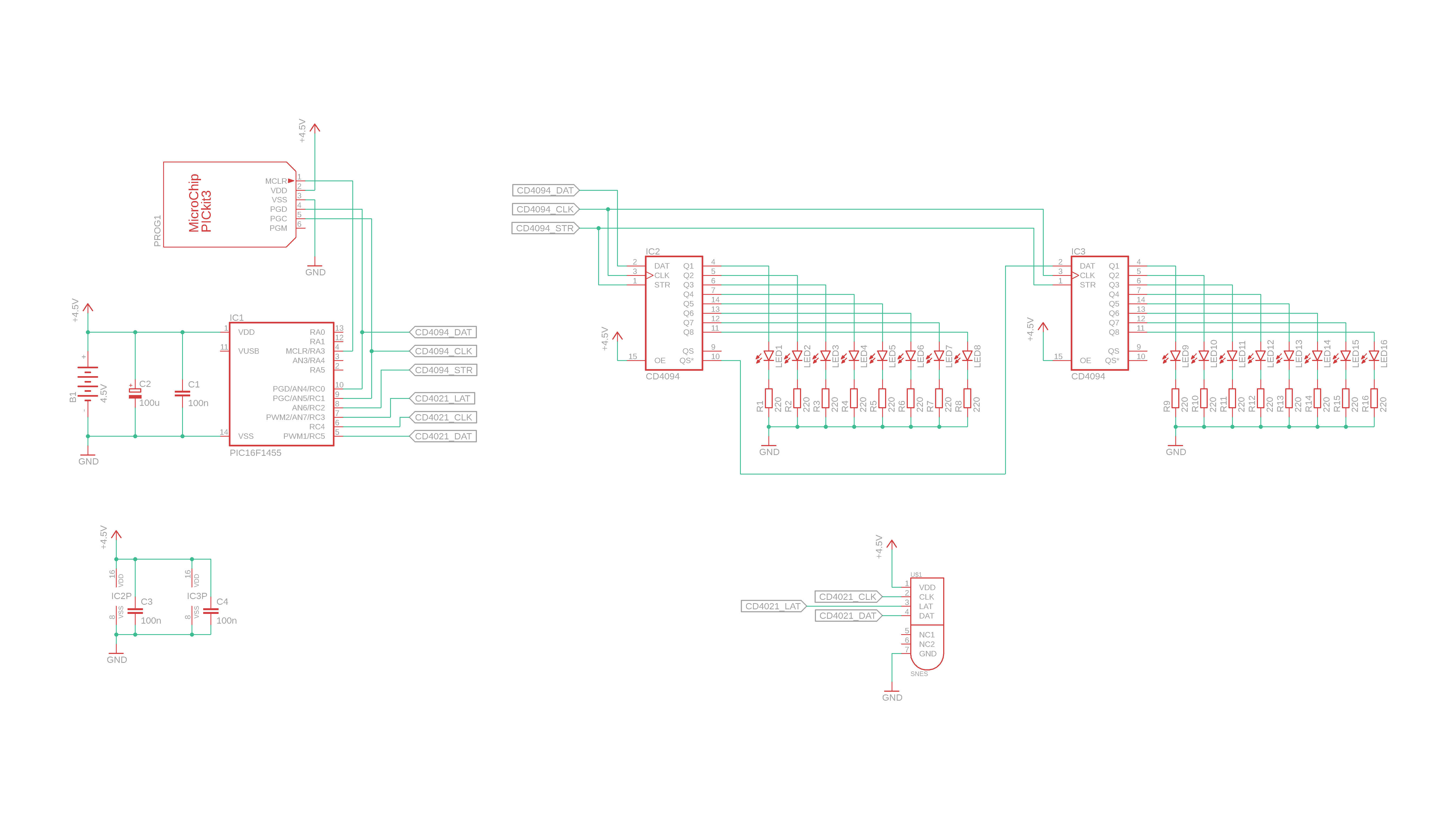
In the middle is the PIC16F1455, connected to the 4.5V battery pack and two capacitors C1 and C2 that stabilize the circuit. The symbol towards the top is the PICkit3 programmer, and it is connected to the circuit with the two power connections VDD and GROUND, and with the three programming connections "master clear," "program data," and "program clock." The little triangle on the PICkit3 sumbol marks the location of the "master clear" pin.
-
-
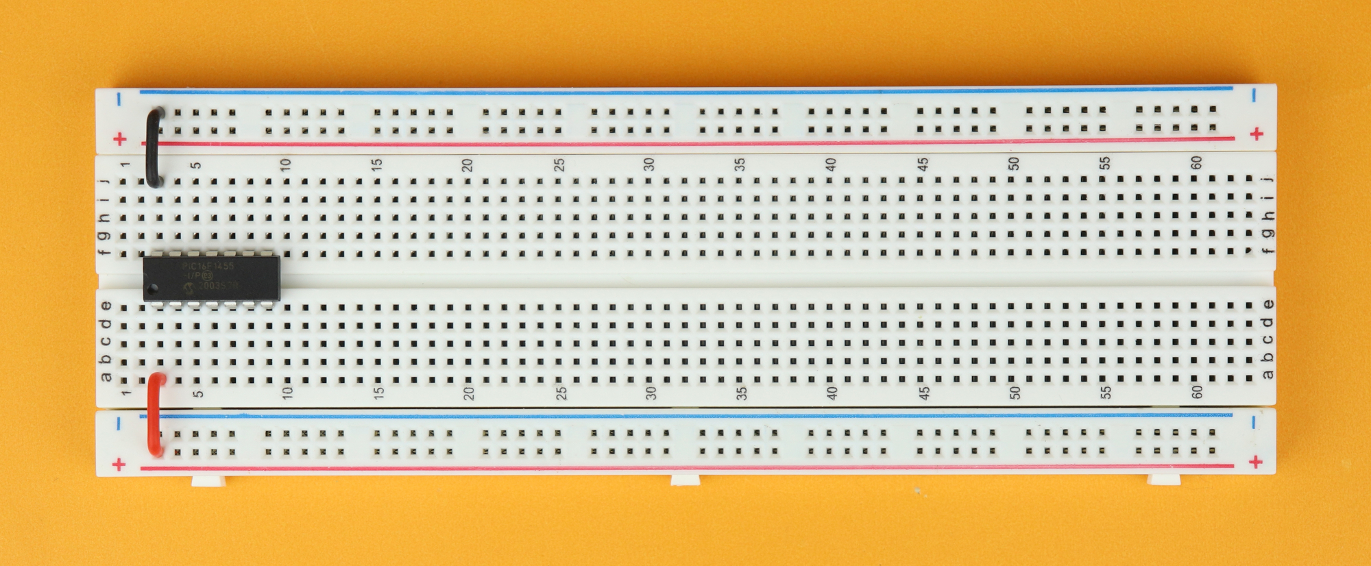
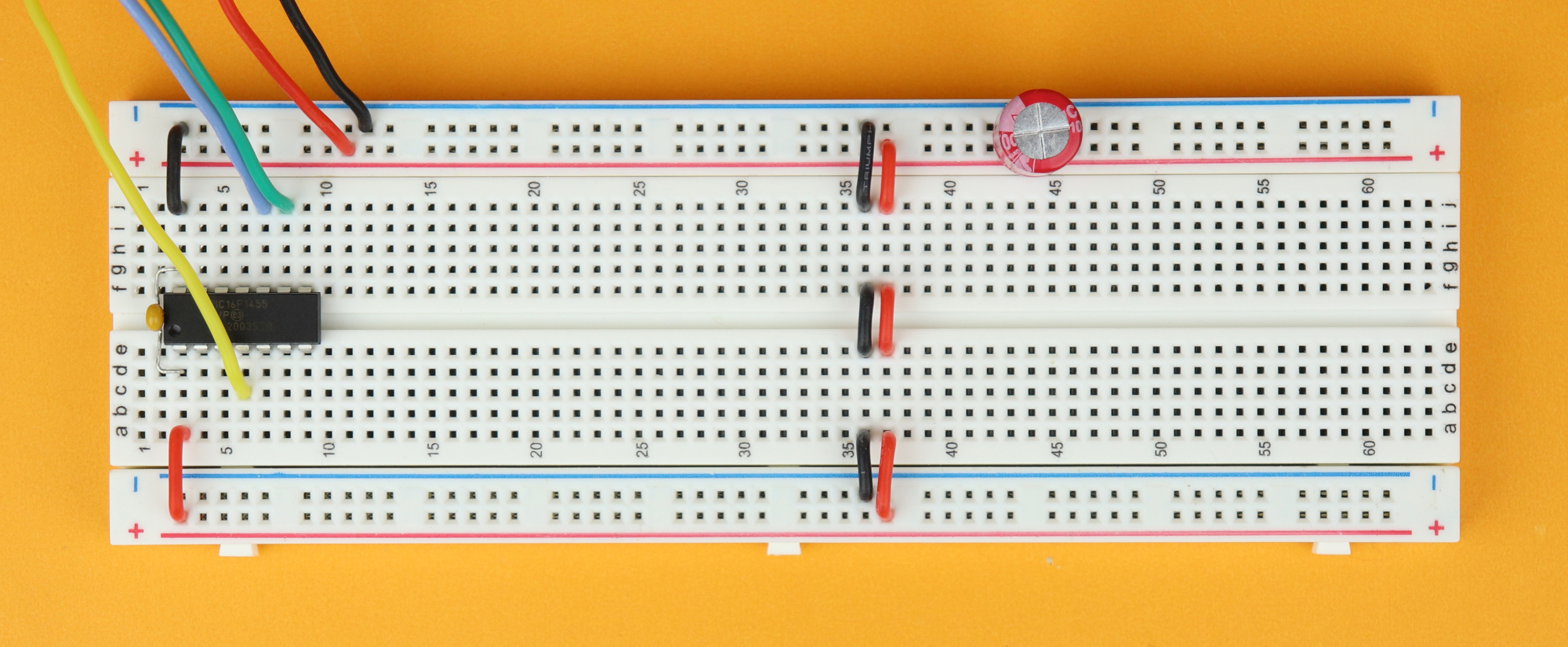
Step 1
Place the breadboard in front of you with row 1 facing to the left. Insert the PIC16F1455 in row 3, with its notch facing to the left. Connect pin 1 to the positive power rail, and pin 14 to the negative power rail.
-
-
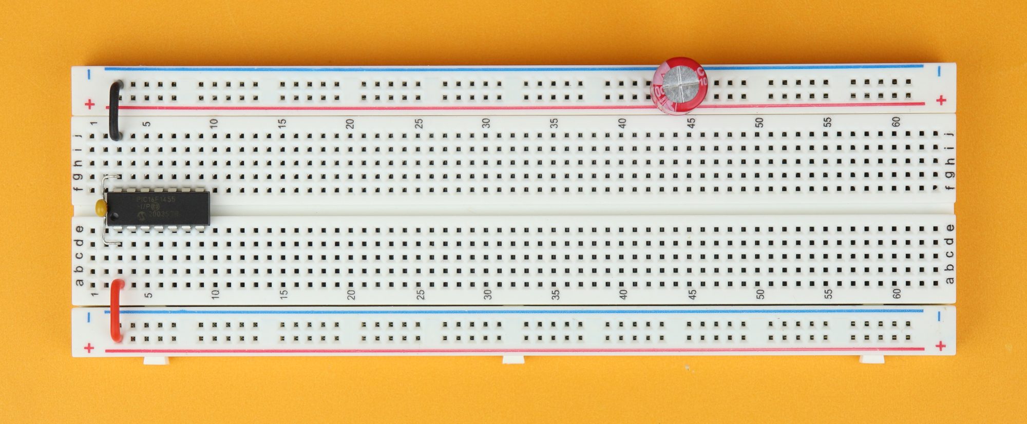
Step 2
Insert the 100nF bypass capacitor C1 between pins 1 and 14 of the PIC16F1455, as close to the chip as possible. This capacitor can be plugged in either way.
And next, insert the 100μF bulk capacitor C2 in the poewr rail close to row 43 (that location makes sure it's not in the way later)
Important: this capacitor has a big minus sign at one of its pis, and make sure that this negative terminal is connected to the negative power rail. Electrolytic capacitors like C2 get damaged when plugged in incorrectly.
-
-
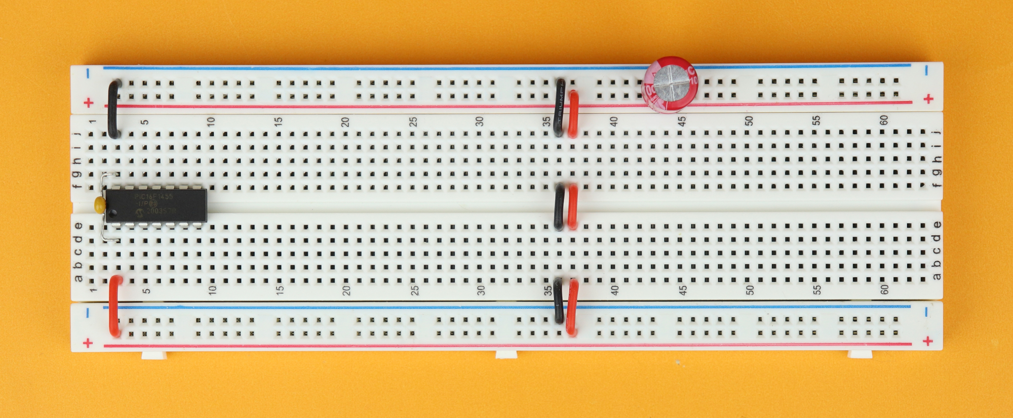
Step 3
Next, make sure that the two positive power rails on either side of the breadboard are connected, and the same for the two negative power rails. Row 36 and 37 are good places for this because this way they won't interfere with what we have planned for later.
-
-
Step 4
Now it's time to connect the PICki3 programmer to our microcontroller.
The power connections VDD (red wire) and GROUND (black wire) can be connected directly to the power rail.
Master clear (yellow wire) is connected to pin 4 of the PIC16F1455, program data (blue wire) goes to pin 10, and program clock (green wire) is connected to pin 9.
Now connect the 4.5V battery pack to the power rail, and plug the PICkit3 into the USB end of your computer. If you are new top this, check out this article on how to use the PICkit3 (or the YouTube video, which you can also find on the article page). After setting up a new project for the PIC16F1455, we can select the configuration bits and code the basic structure of our microcontroller program.
This is how it looks like:
/*
 * File:   main.c
 * Author: boos
 *
 * Created on October 17, 2022, 6:11 PM
 */

// CONFIG1
#pragma config FOSC = INTOSC    // Oscillator Selection Bits (INTOSC oscillator: I/O function on CLKIN pin)
#pragma config WDTE = OFF       // Watchdog Timer Enable (WDT disabled)
#pragma config PWRTE = OFF      // Power-up Timer Enable (PWRT disabled)
#pragma config MCLRE = OFF      // MCLR Pin Function Select (MCLR/VPP pin function is digital input)
#pragma config CP = OFF         // Flash Program Memory Code Protection (Program memory code protection is disabled)
#pragma config BOREN = OFF      // Brown-out Reset Enable (Brown-out Reset disabled)
#pragma config CLKOUTEN = OFF   // Clock Out Enable (CLKOUT function is disabled. I/O or oscillator function on the CLKOUT pin)
#pragma config IESO = OFF       // Internal/External Switchover Mode (Internal/External Switchover Mode is disabled)
#pragma config FCMEN = OFF      // Fail-Safe Clock Monitor Enable (Fail-Safe Clock Monitor is disabled)

// CONFIG2
#pragma config WRT = OFF        // Flash Memory Self-Write Protection (Write protection off)
#pragma config CPUDIV = CLKDIV6 // CPU System Clock Selection Bit (CPU system clock divided by 6)
#pragma config USBLSCLK = 48MHz // USB Low SPeed Clock Selection bit (System clock expects 48 MHz, FS/LS USB CLKENs divide-by is set to 8.)
#pragma config PLLMULT = 3x     // PLL Multipler Selection Bit (3x Output Frequency Selected)
#pragma config PLLEN = ENABLED  // PLL Enable Bit (3x or 4x PLL Enabled)
#pragma config STVREN = ON      // Stack Overflow/Underflow Reset Enable (Stack Overflow or Underflow will cause a Reset)
#pragma config BORV = LO        // Brown-out Reset Voltage Selection (Brown-out Reset Voltage (Vbor), low trip point selected.)
#pragma config LPBOR = OFF      // Low-Power Brown Out Reset (Low-Power BOR is disabled)
#pragma config LVP = OFF        // Low-Voltage Programming Enable (High-voltage on MCLR/VPP must be used for programming)

#include <xc.h>

// main function
void main (void) {

    // main loop
    while (1) {

    }

    return;

}
There is really not a whole lot going on, but that's the point, we are just getting started. Our main program will be contained in the infinite main-loop in row 36. For now we have to compile this code in the MPLAB X IDE, and this is how it looks like:
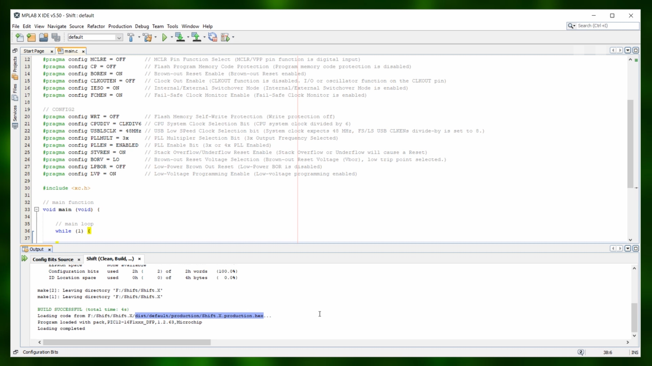
Then we flash the resulting .hex-file onto the PIC16F1455 using the MPLAB IPE:

I know, this sounds all a bit mysterious and terrifying, but it's really not that difficult and you can find all information you could ever want (and more) in the dedicated article. I promise you that it takes less than 20 minutes for you to get set up :)
But after you flash the .hex-file onto the PIC, nothing happens yet, and that is normal because we haven't even connected anything to the PIC16F1455 yet, and the main-loop is still empty. So why did we do all of that? I just like to make sure that our tool chain is working, and that we can reliably compile our code and flash the .hex-file onto the controller. If that works well, we can already exclude this as a potential future error. But it is still a bit boring on the breadboard. So let's change that and add our first CD4094 register!
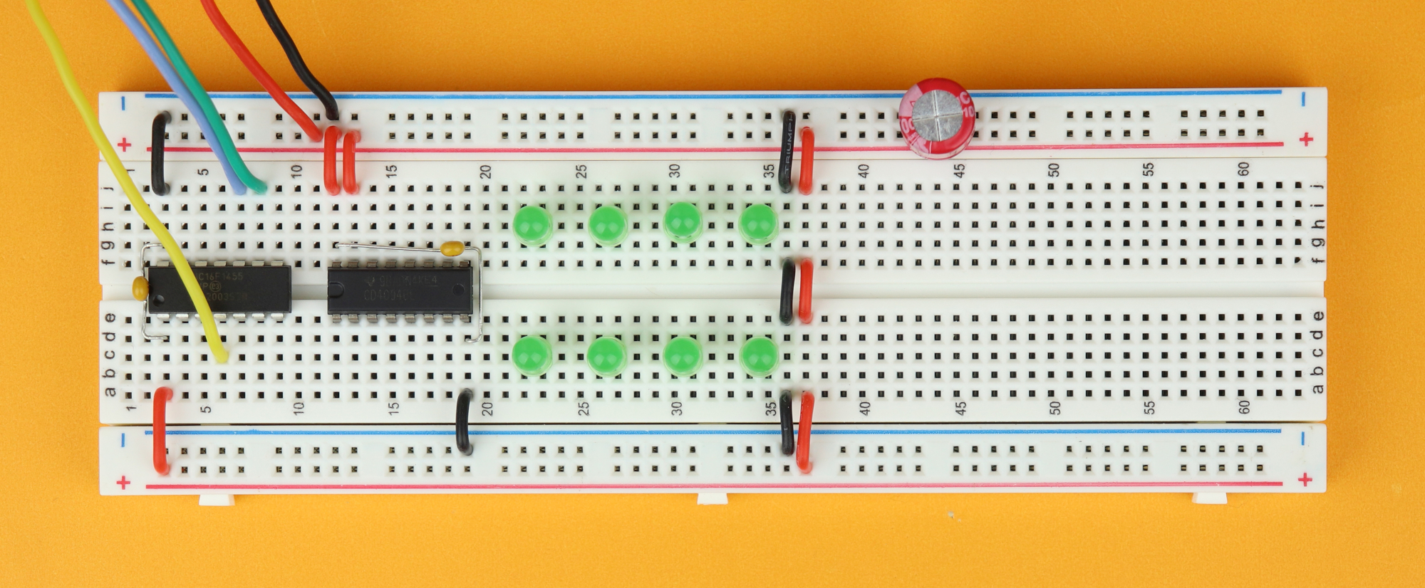
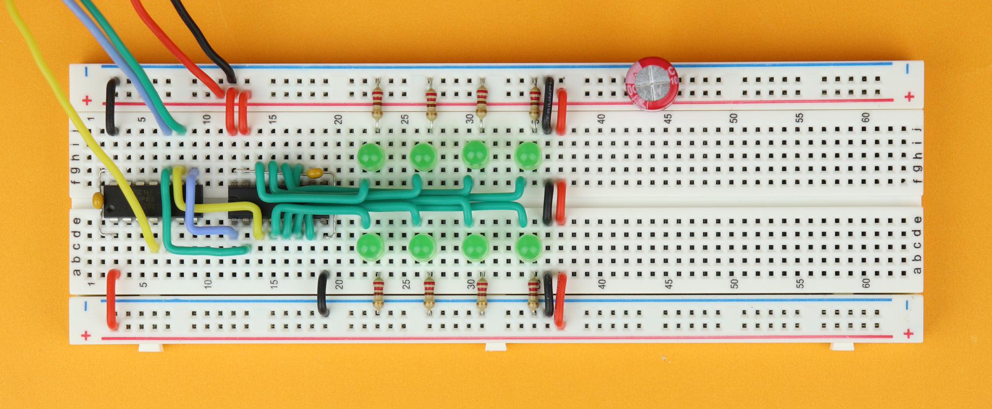
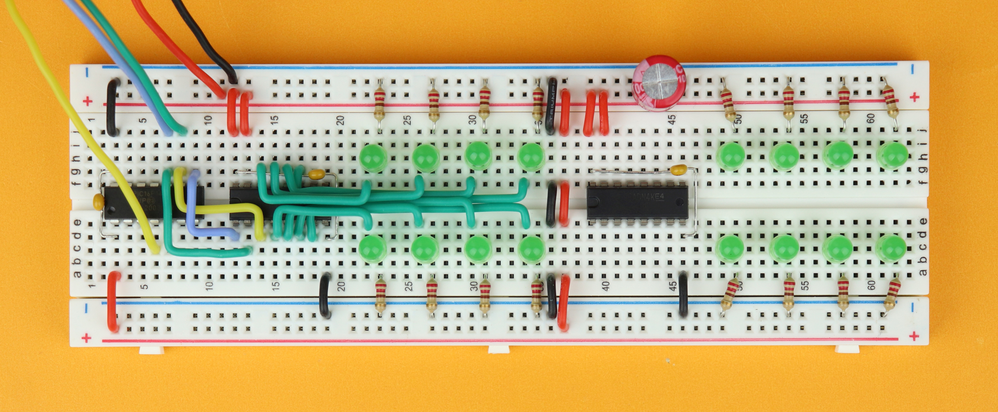
Controlling one CD4094
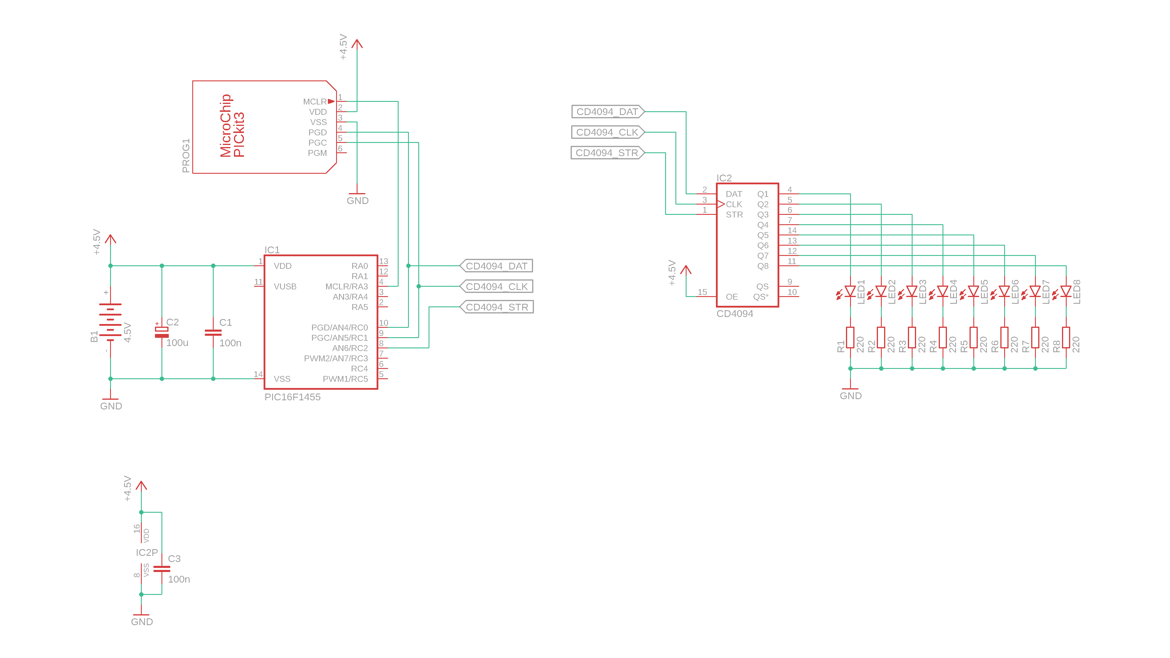
So... here it is! The CD4094 is connected to VDD and GROUND at pins 16 and 8, and it gets a bypass capacitor C3 for stability. Its three inputs DATA, CLOCK, and STROBE are connected to the PIC16F1455 (which makes sense, because we are using the controller to, well, control the CD4094). And its OE input (which stands for OUTPUT ENABLE) is permanently connected to VDD, which just makes sure that its outputs are always active.
Speaking of outputs, here we connect our first eight LEDs, each with a 220Ω with a current-limiting resistor. Keep in mind that the CD4094 is not an LED driver (use the TLC5916 or MAX7219 for that), we are just adding the LEDs here to visualize the logic level of the shift register outputs.
But that's it, on the hardware sind of things. Let's put that on the breadboard, and then worry about modifying our microcontroller program to send out data to those LEDs!
-
-
Step 5
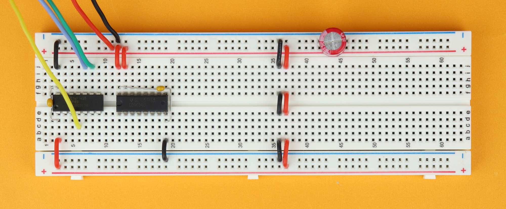
First, disconnect the power. Then, insert the CD4094 in row 12, with its notch pointing to the left.
Connect pin 16 to VDD, pin 8 to ground, and insert the bypass capacitor C3 between pins 16 and 8, as close to the chip as possible. If you do it like in the picture, be careful that the leads of the capacitor do not accidentally short out any of the CD4094's pins.
Connect the output enable input at pin 15 to VDD as well.
-
-
Step 6
Insert the eight LEDs in rows 22, 26, 30, and 34, on either side of the middle breadboard divider. Make sure that the LED cathodes point to the right.
-
-
Step 7
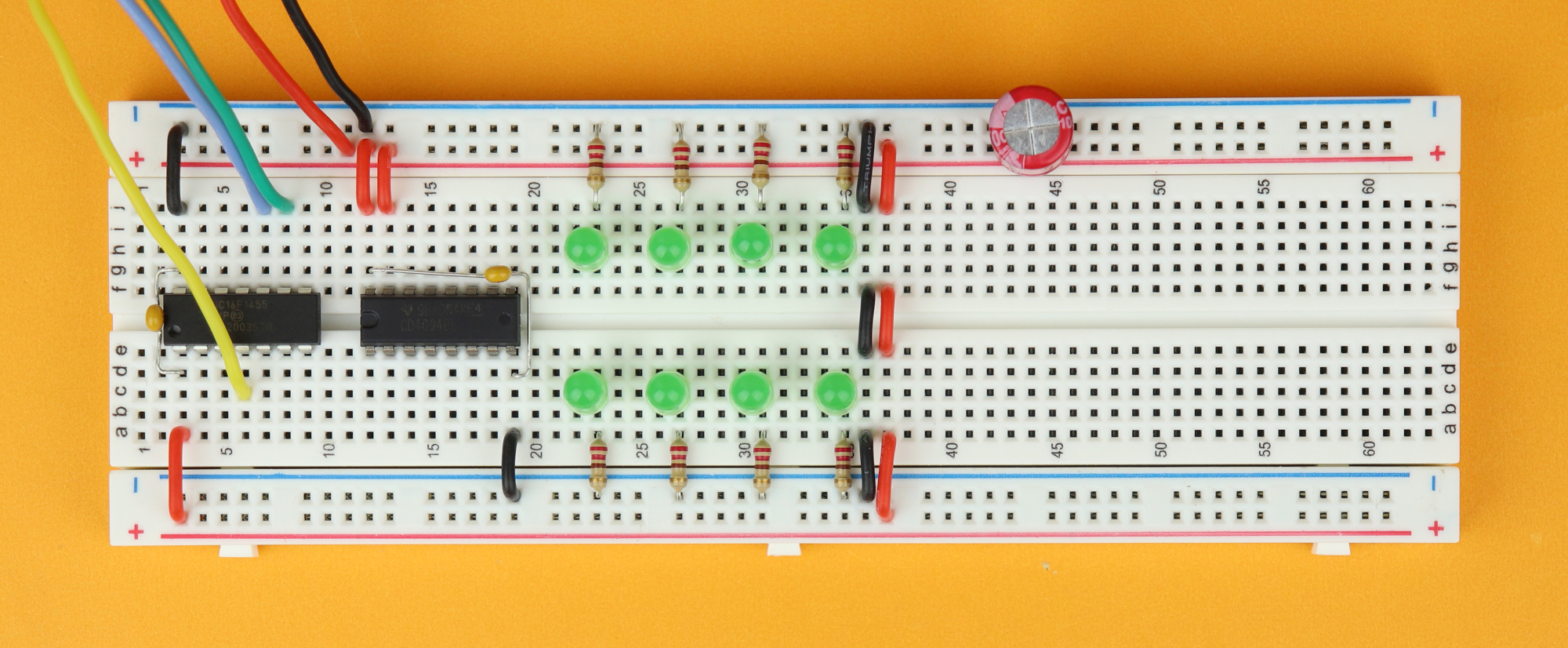
Insert the eight current-limiting resistors between each LED's cathode (on the right) and the ground power rail.
-
-
Step 8
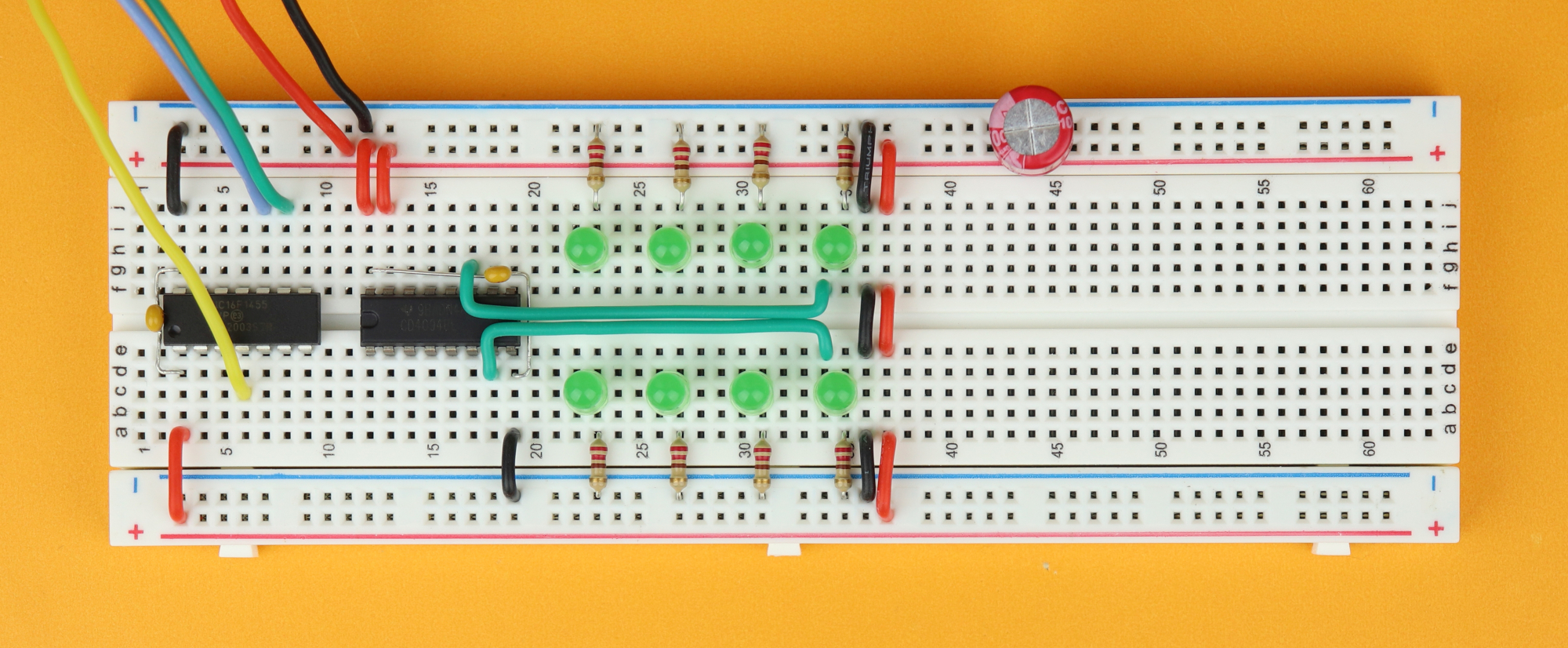
Now it's time to connect the CD4094 outputs to the LEDs. When you do it in pairs, like I will show you here, you can avoid a bit of the mess and it actually won't look that bad.
Connect Q8 at pin 11 to row 34 (upper side of the breadboard), and Q4 at pin 7 to row 34 (lower side of the breadboard).
-
-
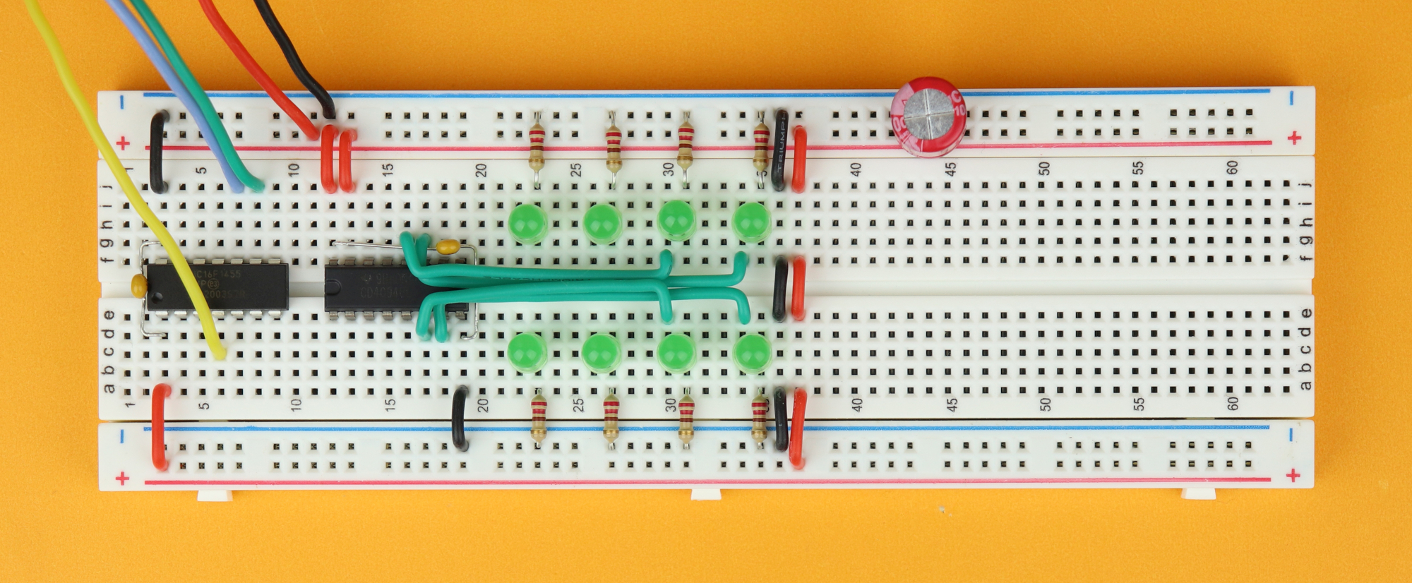
Step 9
Connect Q7 at pin 12 to row 30 (upper side of the breadboard), and Q3 at pin 6 to row 30 (lower side of the breadboard).
-
-
Step 10
Connect Q6 at pin 13 to row 26 (upper side of the breadboard), and Q2 at pin 5 to row 26 (lower side of the breadboard).
-
-
Step 11
Connect Q5 at pin 14 to row 22 (upper side of the breadboard), and Q1 at pin 4 to row 22 (lower side of the breadboard).
-

-
Step 12
Now we can finally connect the CD4094 to the PIC16F1455.
Connect DATA from pin 2 of the CD4094 to pin 10 of the PIC16F1455; CLOCK from pin 3 of the CD4094 to pin 9 of the PIC16F1455; and STROBE from pin 1 of the CD4094 to pin 8 of the PIC16F1455.
-
-
Step 13
And now plug the power back in.
And now that this is all built, let's think about how to get some data out to our LEDs.
// define functions
void CD4094_send (unsigned char b);
void CD4094_load (void);

// abbreviations for convenience
#define CD4094_DAT RC0
#define CD4094_CLK RC1
#define CD4094_STR RC2- First, I like to use the
#define-command to, well, define the locations for DATA, CLOCK, and STROBE. This is optional, but I think it makes the code a bit more readable later on. And because we will have a DATA and CLOCK line for the CD4021 later as well, I called the pinsCD4094_DAT(data),CD4094_CLK(clock), andCD4094_STR(strobe). - In lines 33-34 we define two functions that we will use to send out data, more on those in just a bit!
// main function
void main (void) {


    // set up ports RC0:2 as outputs
    TRISC0 = 0;
    TRISC1 = 0;
    TRISC2 = 0;

	// disable analog features on ports RC0, RC1, and RC2
    ANSC0 = 0;
    ANSC1 = 0;
    ANSC2 = 0;


    // main loop
    while (1) {

		// send out some information
		CD4094_send(0b11000001);
        CD4094_load();

    }

    return;

}- Inside the main function, we should first make sure that our outputs (data, clock, and strobe) are relly outputs (lines 46-48).
- After that, we also have to disable all analog features on those pins. This can be a bit annoying, especially when you are getting started, but unfortunately there is no easy way around it. Anyway, lines 51-53 turn off the analog-to-digital converter functionality on pins RC0, RC1, and RC2.
- And then, inside the main-loop, we send out the byte
0b11000001to the CD4094 with ourCD4094_send()-function, which takes whatever byte we want to send as an argument. This byte is of course just an argument, and each one of those 1's and 0's corresponds to what each of our eight LEDs will show on the CD4094 outputs. - And, finally, we have to pulse the strobe output, to make sure our data also shows up on the CD4094's outputs. And I opted to make this a separate function, which is more useful in our case as we will see later.
// This function sends a byte "b" to the CD4094
void CD4094_send (unsigned char b) {

    // send out all eight bits
    for (int i=7; i>=0; i--) {
        CD4094_DAT = (b >> i) & 1;
        CD4094_CLK = 1;
        CD4094_CLK = 0;
    }

}- And this is where the magic happens! Inside the
CD4094_send()-function, we send out the bytebto the CD4094. The for-loop in line 73 cycles through the eight bits of our byte, and in line 74 we extract the i-th bit. If you want to learn more about those types of bit-manipulating operations, check out the binary numbers article. - So, for each bit, we put it on the data output in line 74, and then pulse the clock output in lines 75-76. And that's it!
// This function refreshes the status of all CD4094 outputs
void CD4094_load (void) {

    // read the status of all CD4021 inputs
    CD4094_STR = 1;
    CD4094_STR = 0;

}- And the
CD4094_load()-function is very simple, it really just pulses the strobe output.
And after you compile the source code and flash the .hex-file onto the controller, this is what you should see:
And here is how that corresponds to our code:
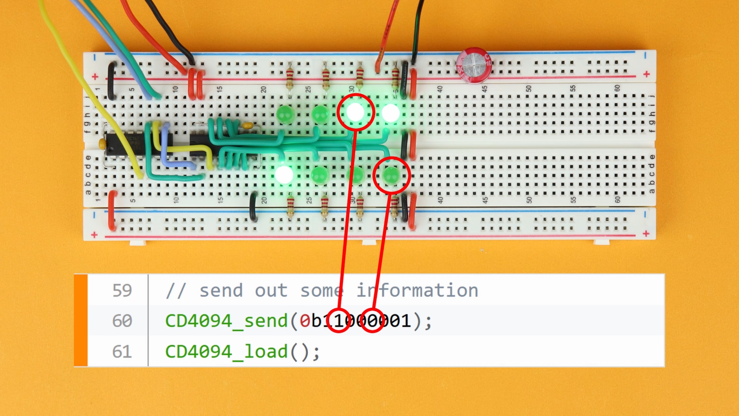
The circled 1 is bit number 7, and corresponds to output Q7; the circled 0 is bit number 4, and corresponds to output Q4. Think about this for a little, because it is a bit confusing at first. Or, better yet, program it yourself and change the 1's and 0's in row 60, and send out different patterns! For example, instead of the eight LEDs you could connect a 7-segment display and send out all kinds of symbols!
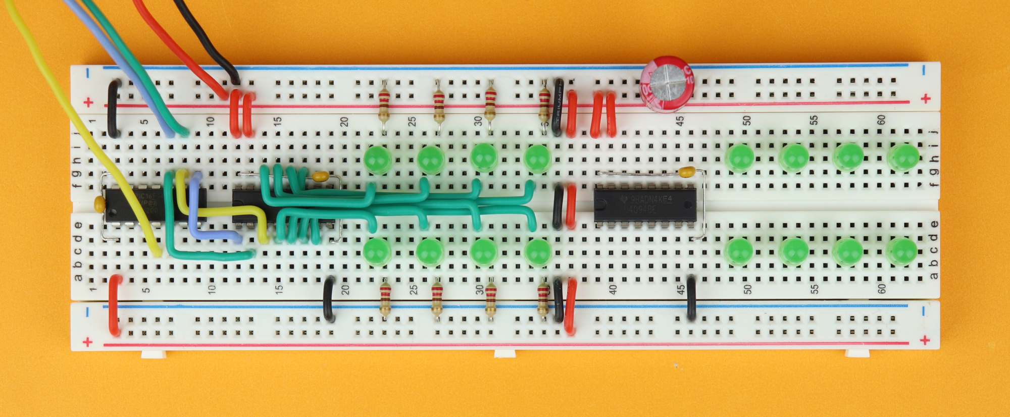
Adding one more CD4094
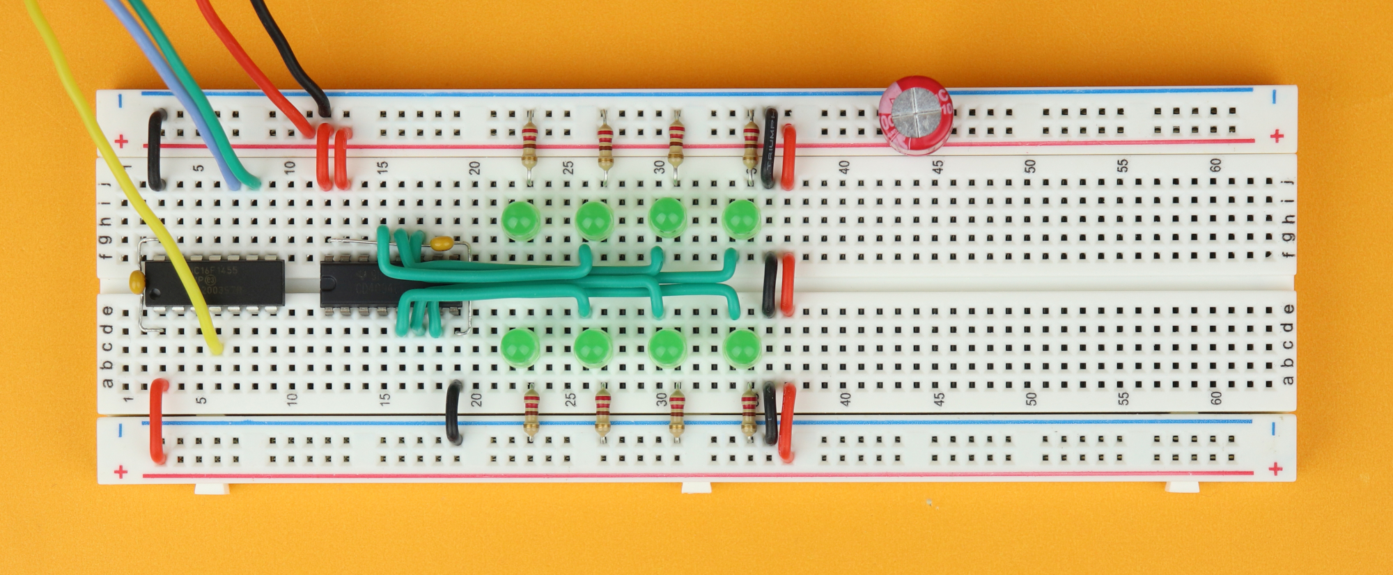
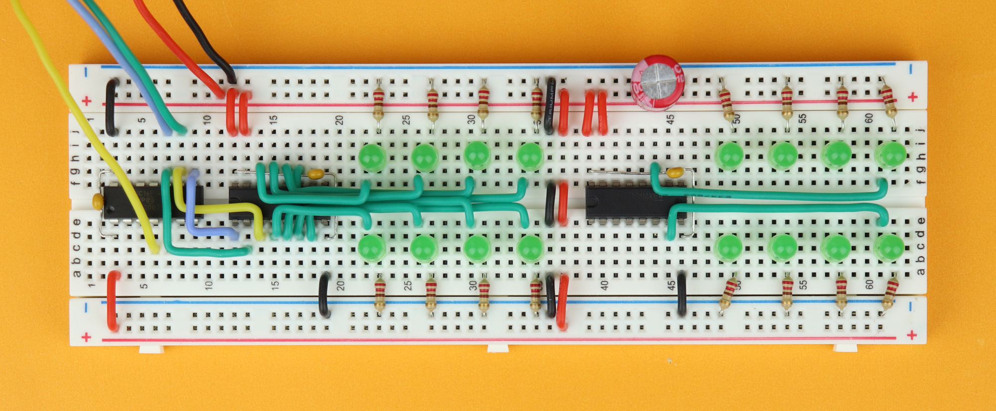
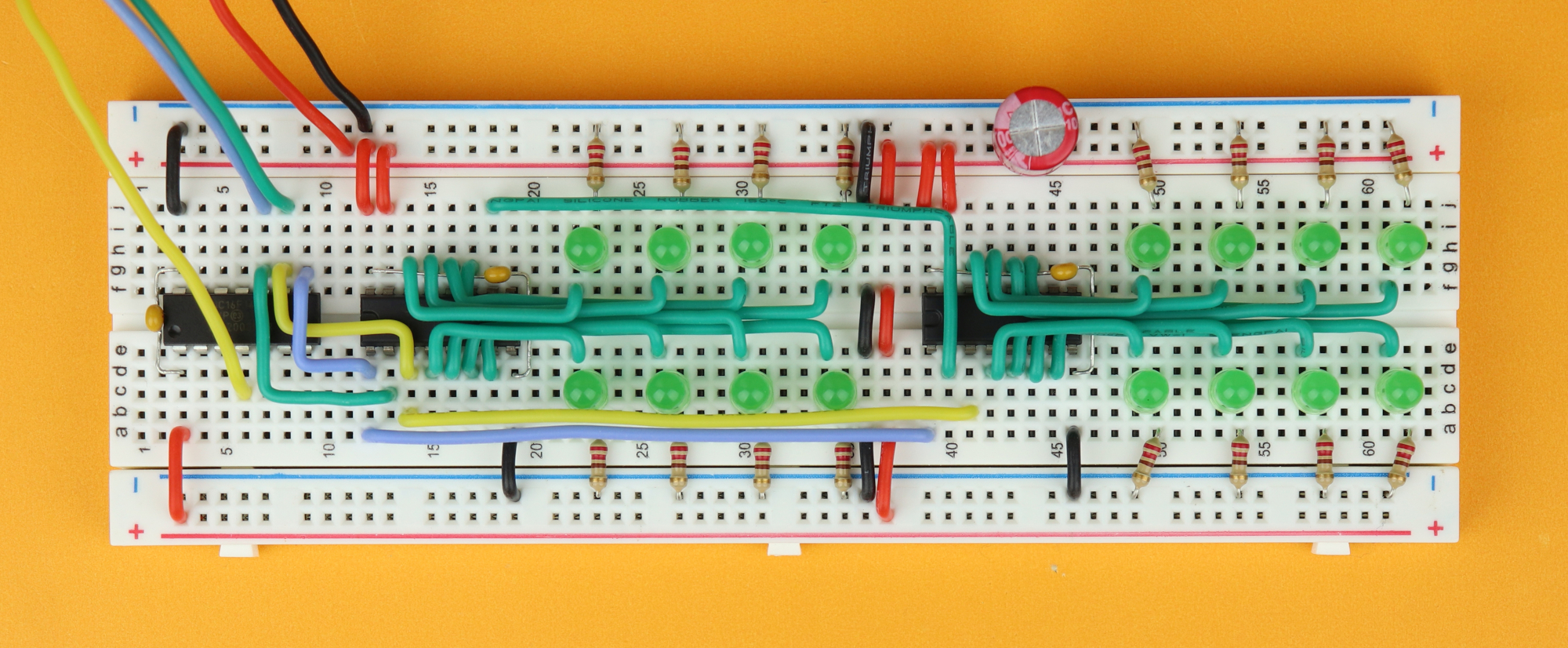
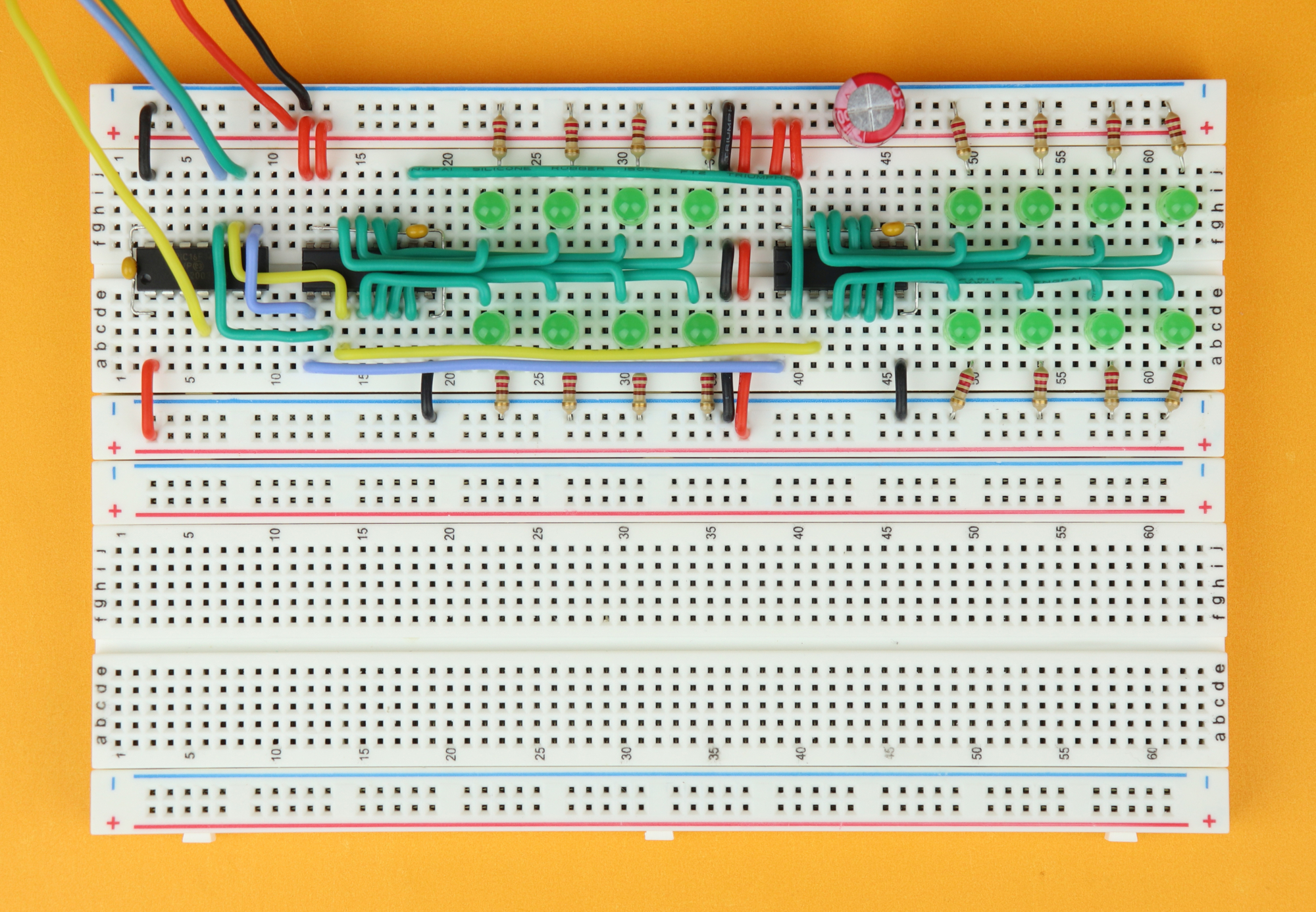
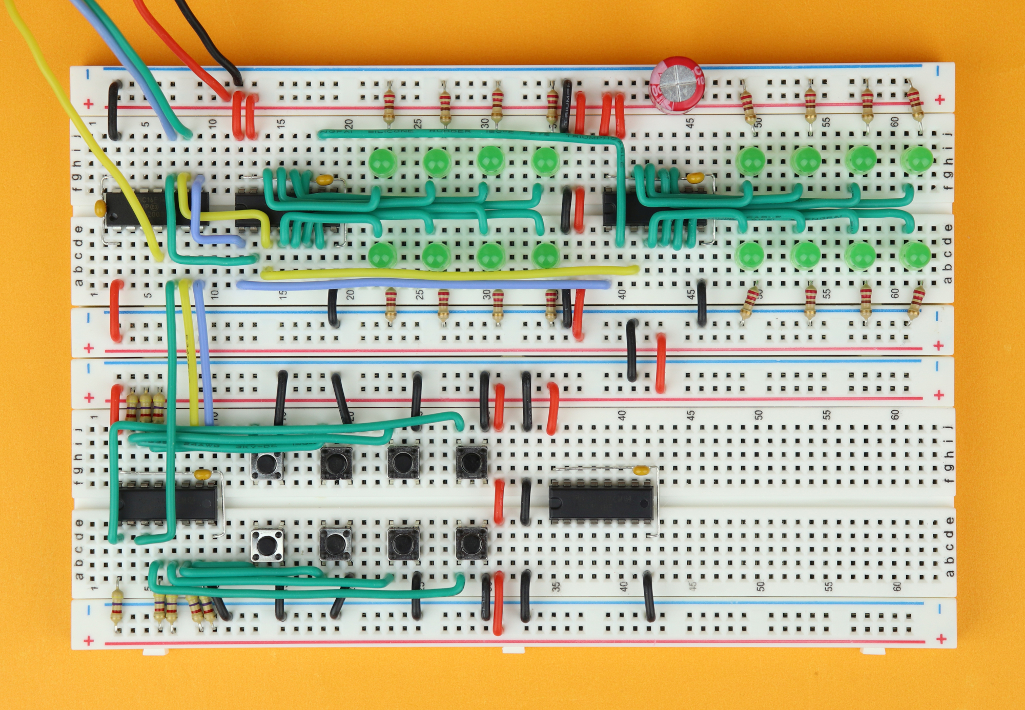
Do you know what's better than one CD4094? Two CD4094! And here is how that looks like:
It's really not that difficult: for starters, the VDD and GROUND connections are exactly the same as before, and we also add eight LEDs on the outputs. Moreover, CLOCK and STROBE are connected in parallel.
So what is different? It's only the DATA input. It is not connected to the PIC, but rather to the Q'S output of the previopus CD4094 (IC2). This way it takes the data that “falls out of” the first CD4094 and keeps it alive.
The really nice feature of this is that we do not need any additional wires at the PIC16F1455, we are building a chain! In a similar way you could add more CD4094's, and they could be as many as you want. Okay, but for today, we will call it ad two CD4094's because the wiring becomes more and more work. Let's do that next!
-
-
Step 14
First, disconnect the power.
-

-
Step 15
Then, insert the CD4094 in row 39, with its notch pointing to the left.
Connect pin 16 to VDD, pin 8 to ground, and insert the bypass capacitor C3 between pins 16 and 8, as close to the chip as possible. If you do it like in the picture, be careful that the leads of the capacitor do not accidentally short out any of the CD4094's pins.
Connect the output enable input at pin 15 to VDD as well.
-
-
Step 16
Insert the other eight LEDs in rows 49, 53, 57, and 61, on either side of the middle breadboard divider. Make sure that the LED cathodes point to the right.
-
-
Step 17
Insert the eight current-limiting resistors between each LED's cathode (on the right) and the ground power rail.
-
-
Step 18
Now it's time to connect the CD4094 outputs to the LEDs. And again, when you do it in pairs you can avoid a bit of the mess.
Connect Q8 at pin 11 to row 61 (upper side of the breadboard), and Q4 at pin 7 to row 61 (lower side of the breadboard).
-
-
Step 19
Connect Q7 at pin 12 to row 57 (upper side of the breadboard), and Q3 at pin 6 to row 57 (lower side of the breadboard).
-

-
Step 20
Connect Q6 at pin 13 to row 53 (upper side of the breadboard), and Q2 at pin 5 to row 53 (lower side of the breadboard).
-
-
Step 21
Connect Q5 at pin 14 to row 49 (upper side of the breadboard), and Q1 at pin 4 to row 49 (lower side of the breadboard).
-
-
Step 22
Now we can finally connect this CD4094 to the previous CD4094.
Connect CLOCK from pin 3 of this CD4094 (in row 41) to pin 3 of the previous CD4094 (in row 14); and connect STROBE from pin 1 of this CD4094 (in row 39) to pin 1 of the previous CD4094 (in row 12).
And, last, connect DATA at pin 2 of this CD4094 (in row 40) to the Q'S output of the previous CD4094 in row 18 (upper half of the breadboard).
-
-
Step 23
And, finally, plug the power back in.
And in our program from before, we now only need to add one extra line:
// main loop
while (1) {
// send out some information
CD4094_send(0b10001000);
CD4094_send(0b11110000);
CD4094_load();
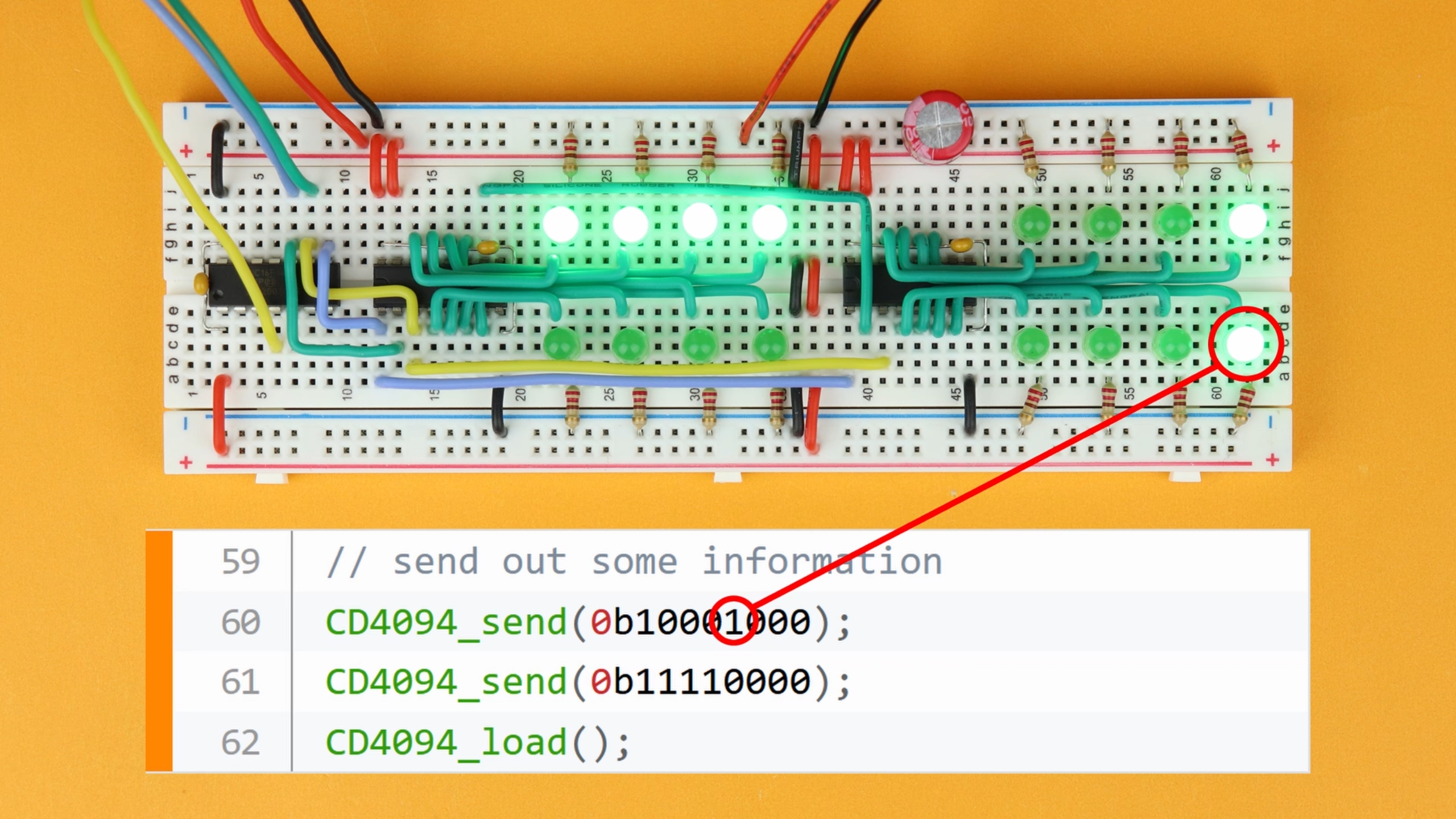
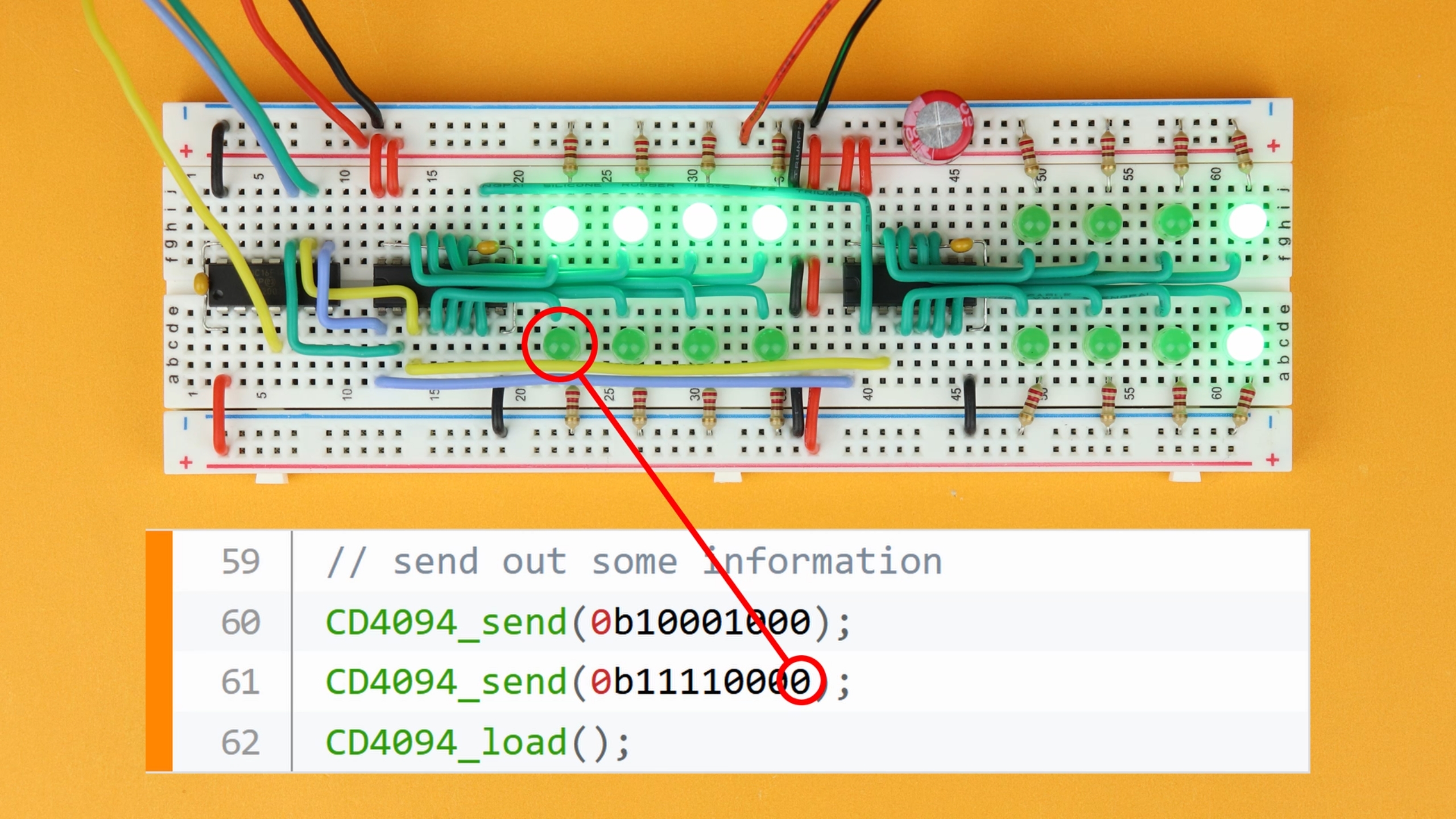
}And that's it! You can see that the first line (line 60) gets sent out first, so this display pattern reaches the second set of eight LEDs. This sounds a bit odd at first, but it makes total sense because this is the data that is sent out first, so it travels down our chain the farthest.
The second line (line 61) is sent out after. And, for the same reason as above, this pattern shows up on the first set of LEDs.
Here is how that looks like:
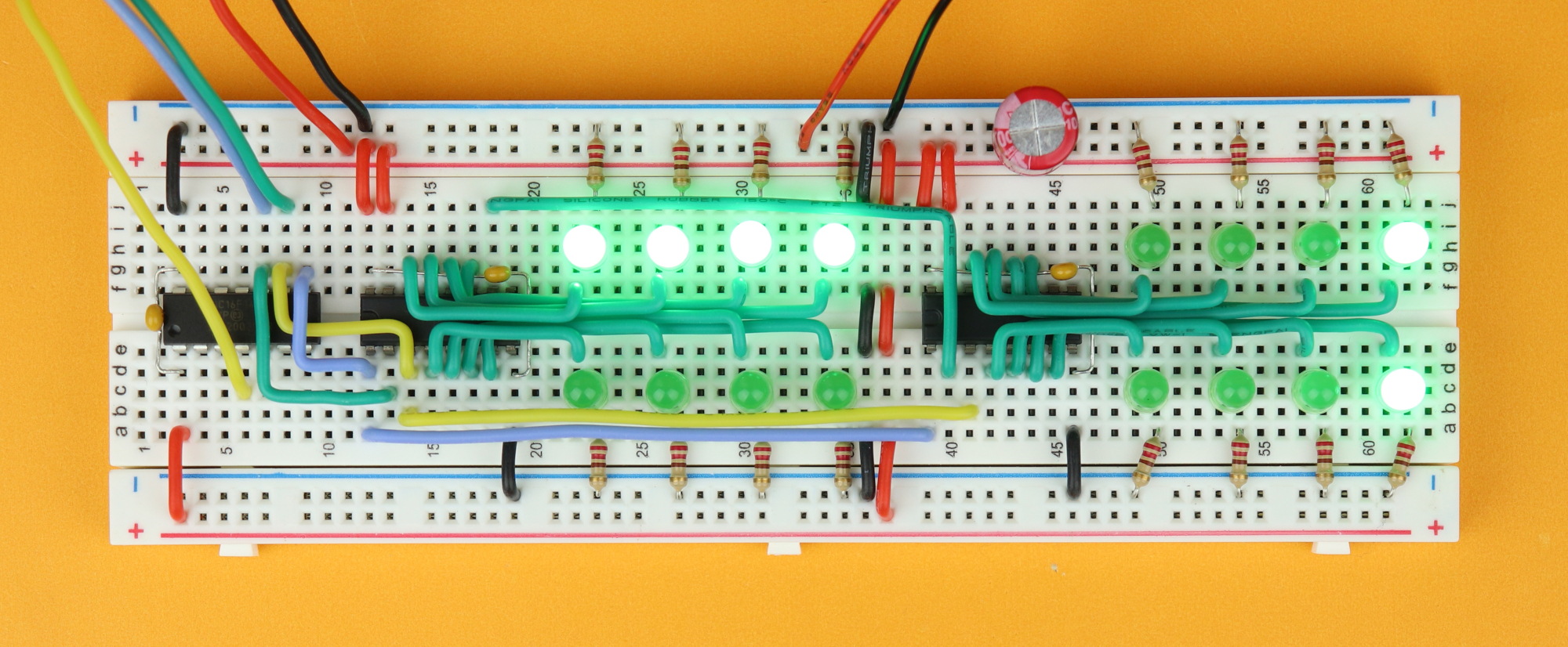
And here you can see a one-to-one comparison of some of the bits:
At this point it is already becoming more useful. Adding two additional CD4094's, for example, you could arelady build a 7-segment clock! But I think you get the idea. So let's now move on to reading out pushbuttons!
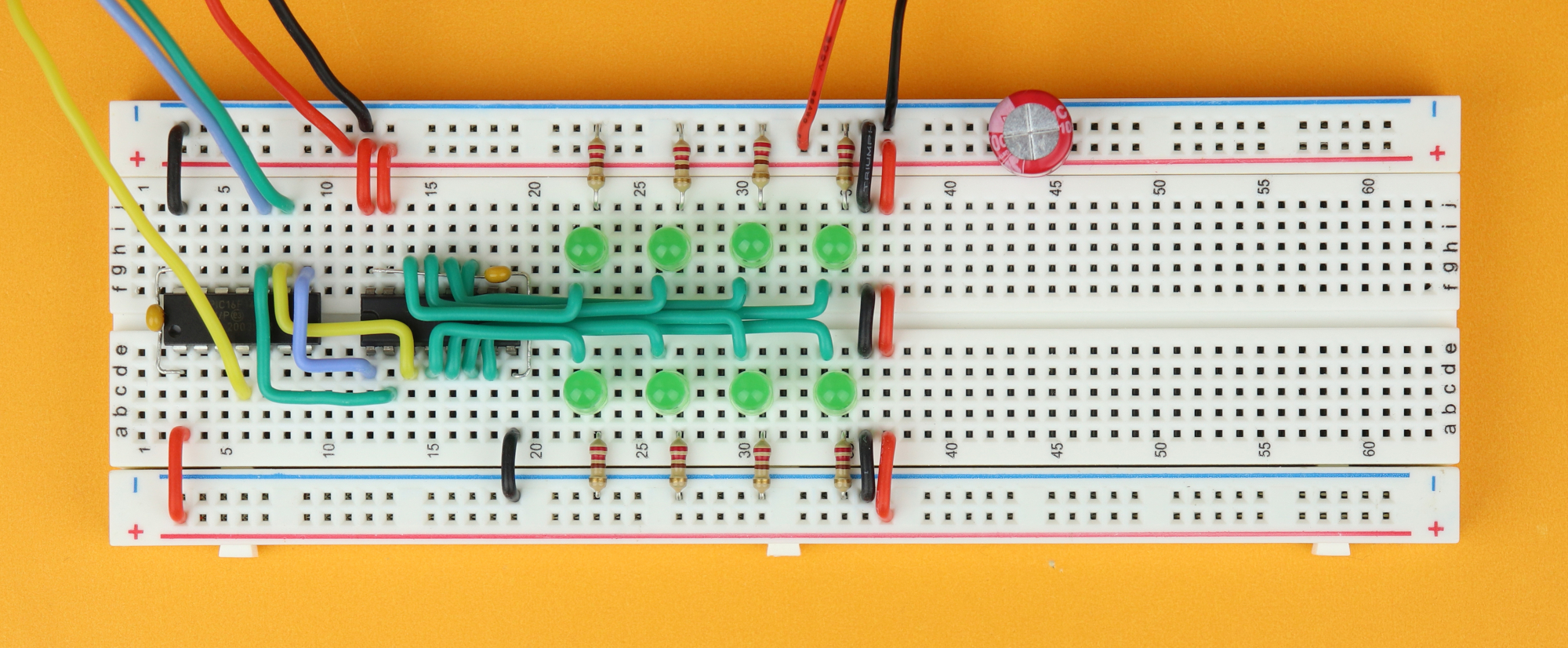
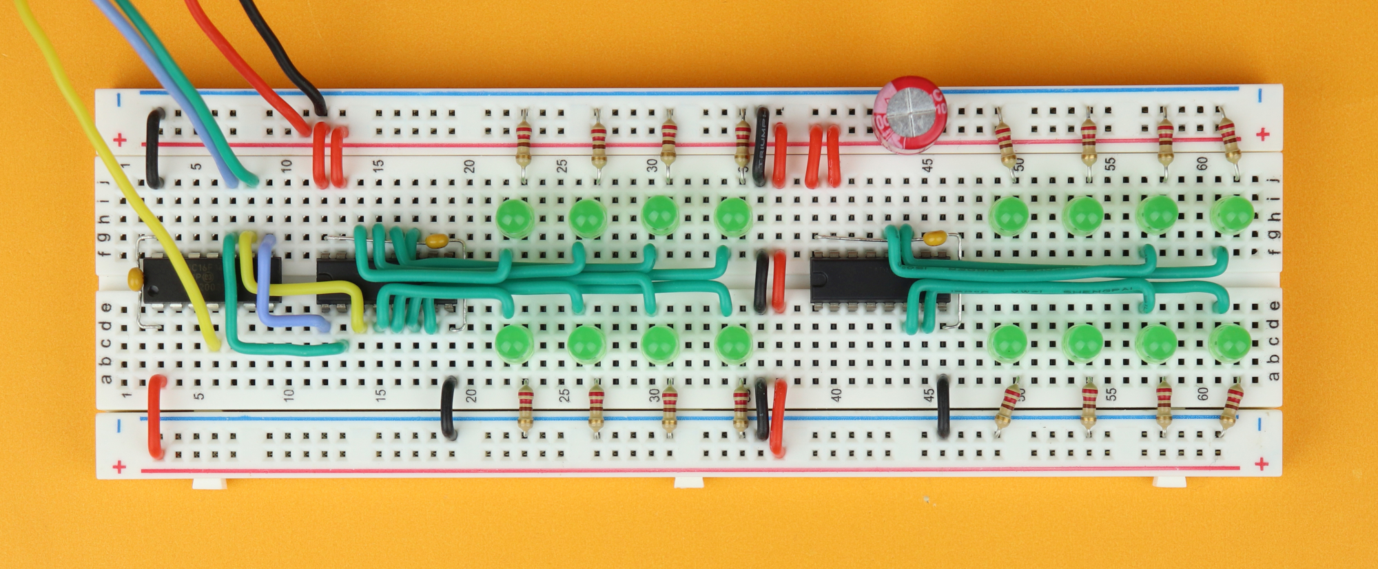
Reading out one CD4021
So let's s tart with just one CD4021 at first:
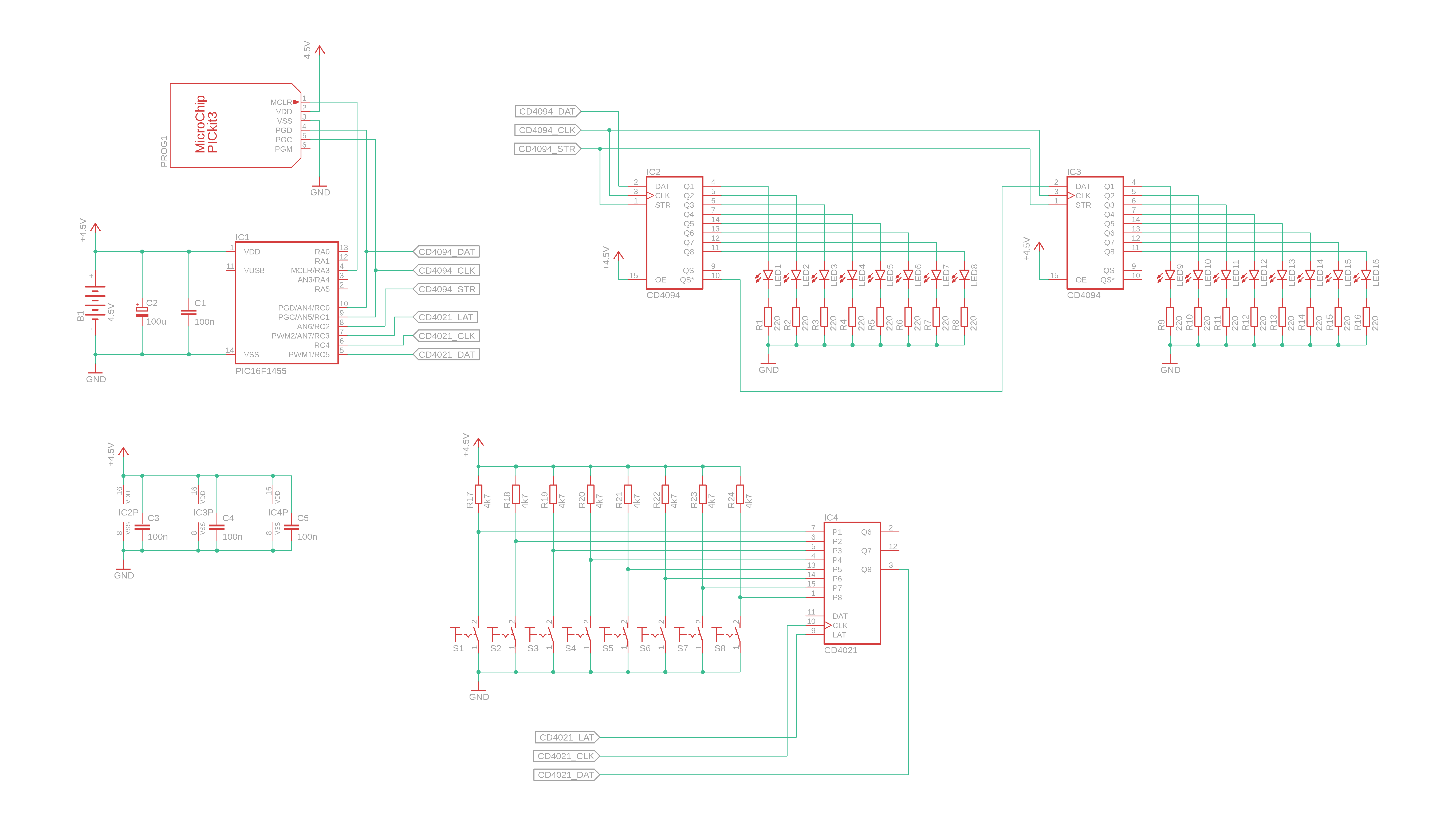
The power is connected to the CD4021 at pins 16 and 8, and we again add a bypass capacitor for stability. Each CD4021 input (P1-P8) is connected to ground via a pushbutton, and to VDD with a 4.7kΩ pullup resistor. This way, each input is a logical 1 when the button is deactivated, and a logical 0 when the button is active. This inverts the logic (a 0 means the button is pressed, and a 1 means that the button is not doing anything) but this configuration has the advantage that the current that flows into the CD4021's inputs is automatically limited by the pullup resistors.
Okay, but how do we read out the data? Just as before, CLOCK is connected to the PIC16F1455 in a separate wire, and so is the LATCH pin (which is the same as the STROBE pin for the CD4094). This part is easy. What about the DATA pin? Why is it not connected?
Remember that we are trying to read out data, not send it. So we have to connect the Q8 output of the CD4021 to the PIC16F1455, and that's exactly what we are doing here. We will make use of the DATA input of the Cd4021 in the next section, so no worries, I hope it will become clear then.
Alright, let's build this!
-
-
Step 24
Since we have officially run out of space, add a second breadboard at the bottom.
-

-
Step 25
Make sure the power rails are connected all the way through.
-
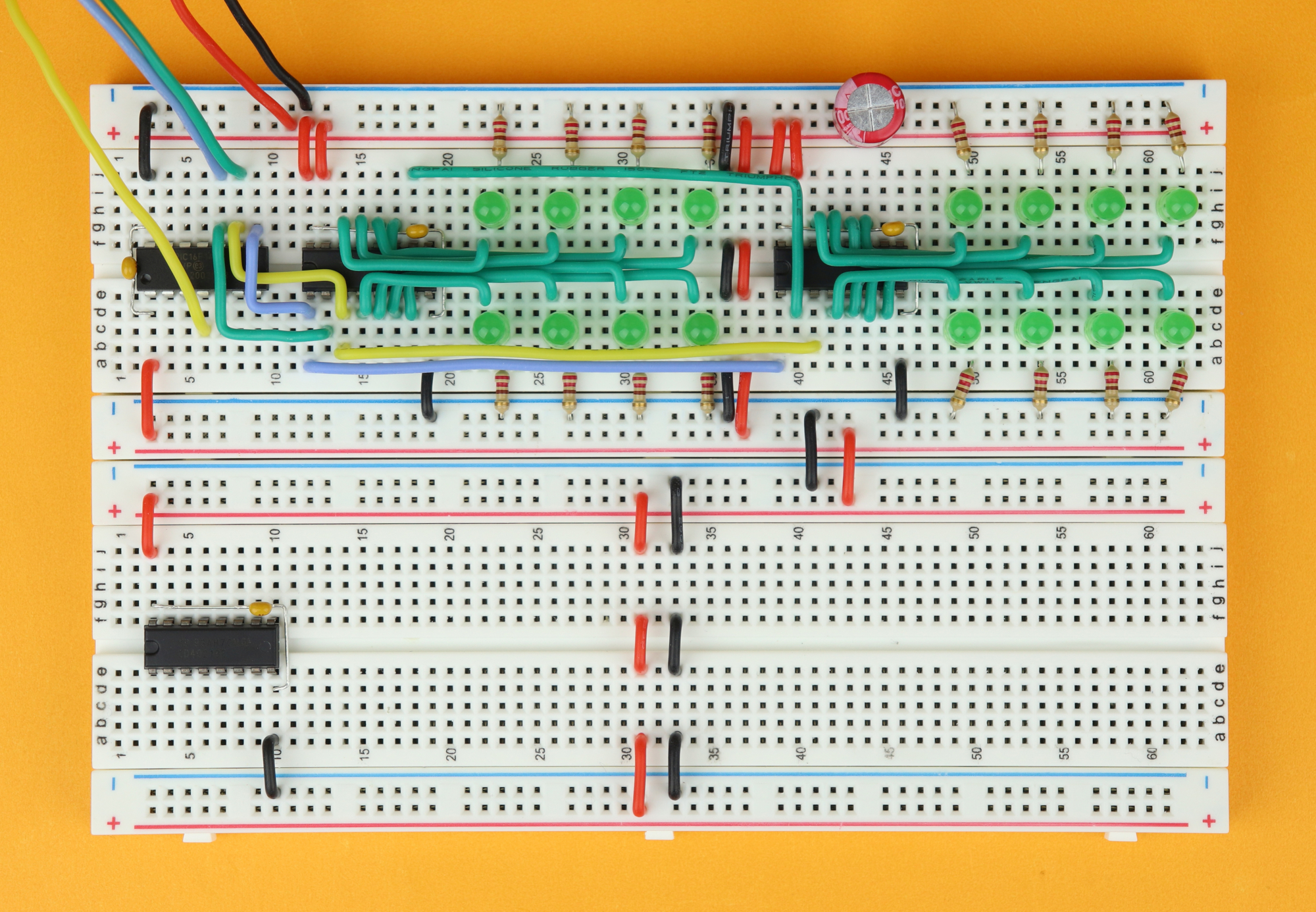
-
Step 26
Insert the CD4021 in row 3 and make sure its notch points to the left. Connect VDD at pin 16 and GROUND on pin 8, and insert the 100nF bypass capacitor C4 between pins 16 and 8, close to the chip.
-
-
Step 27
Insert eight pushbuttons in rows 13, 18, 23, and 28, both on the upper and the lower part of the breadboard.
Important: Make sure you plug in the buttons exactly as in the picture, and don't rotate them by 90 degrees accidentally.
-
-
Step 28
Insert the 4.7kΩ pullup resistors R17–R24 from the P1–P8 inputs of the CD4021 to VDD (pins 1, 4, 5, 6, 7, 13, 14, and 15).
-

-
Step 29
Connect the right terminal of each pushbutton to the ground rail.
-
-
Step 30
Now it's time to connect the other terminal to the CD4021 inputs as well, and it works out nicely if you do it in pairs again.
Connect P1 at pin 7 to row 13 (lower part of breadboard) and P5 at pin 13 to row 13 (upper part of breadboard).
-
-
Step 31
Connect P2 at pin 6 to row 18 (lower part of breadboard) and P6 at pin 14 to row 18 (upper part of breadboard).
-

-
Step 32
Connect P3 at pin 5 to row 23 (lower part of breadboard) and P7 at pin 15 to row 23 (upper part of breadboard).
-
-
Step 33
Connect P4 at pin 4 to row 28 (lower part of breadboard), and, last, P8 at pin 1 (lower part of breadboard) to row 28 on the upper part of the breadboard.
-
-
Step 34
Now it's time to connect the CD4021 to the PIC6F1455. This is a bit difficult to describe in words because it's a connection between the lower and upper breadboard, so also make sure to have a close look at the picture :)
DATA (green wire) goes from pin 5 of the PIC16F1455 to pin 3 of the CD4021; CLOCK (yellow wire) goes from pin 6 of the PIC16F1455 to pin 10 of the CD4021; and STROBE (blue wire) goes from pin 7 of the PIC16F1455 to pin 9 of the CD4021.
-

-
Step 35
And last, plug the power back in.
So let's now write the next part of our program that reads out the status of our eight pushbuttons!
// define functions
void CD4094_send (unsigned char d);
void CD4094_load (void);
unsigned char CD4021_read (void);
void CD4021_load (void);- Here we just added two more functions:
CD4021_read(), which returns the 8-bit value of the pushbuttons, andCD4021_load(), which loads the status of each button into the registers. - When I am using more than one chip as hardware, I like to give functions a prefix (such as CD4094 or CD4021), it makes it more clear to me what is happening when I am reading my own code a few years later.
// input values
unsigned char v1 = 0;- This variable will store our eight bits that we read out from the pushbuttons, more on that later.
// main loop
    while (1) {

        // read out 8 buttons (one byte)
        CD4021_load();
        v1 = CD4021_read();

		// send out the information
		// (invert each bit for the second register, for fun)
		CD4094_send(v1);
        CD4094_send(~v1);
        CD4094_load();

}- And here is our main-loop, in all it's glory: first we read out the pushbutton information, and then pass it along to the LEDs.
- In line 74, we pulse the LATCH-line, which means that the status of all pushbuttons is transferred into the CD4021 registar.
- Then, in line 75, we retrieve these bits with our
CD4021_read()-function, and store the result inv1. - And now we can take that value and send it to our LEDs, which is exactly what line 79 does.
- And in line 80 we send out the inverted information (basically each bit is flipped around, digit by digit, that is what the little tilde does).
- Line 81 finally calls the
CD4094_load()-function that pulses the STROBE line, and the data we just sent out appears on the LEDs.
// This function reads out a byte "b" from the CD4021
unsigned char CD4021_read (void) {

    // initialize the future return value to 0
    unsigned char b = 0;

    // read out all eight bits
    for (int i=7; i>=0; i--) {
        b |= (CD4021_DAT << i);
        CD4021_CLK = 1;
        CD4021_CLK = 0;
    }

    // return the byte
    return b;

}- This function reads out the status of all eight pushbuttons, and it is a bit more complicated, but no worries, we will get there.
- In line 111 we declare this function to return a value, which is why we write
unsigned char CD4021_loadinstead ofvoid CD4021_load. - Then, in line 114, we declare a one-byte variable that will contain the final result (the status of each one of our eight pushbuttons).
- The for-loop starting in line 117 cycles through all eight bits. At each position it reads out whatever signal is on our DATA input, and puts that information to the i-th position inside the byte b (line 118).
- Then we pulse the CLOCK line, and read out the next bit, and so on.
- And, finally, in line 124, we return the result.
// This function loads the status of all CD4021 inputs
void CD4021_load (void) {

    // read the status of all CD4021 inputs
    CD4021_LAT = 1;
    CD4021_LAT = 0;

}- The
CD4021_load()-function is really simple, it just pulses the LATCH line. - You may have notices that for the CD4021 we need to call the load()-function before reading out all information (see lines 74-75 above), but for the CD4094 we call the load()-function after we have sent all the data (see lines 79-81). This can be a bit confusing and a source for errors, so I wanted to mention it here.
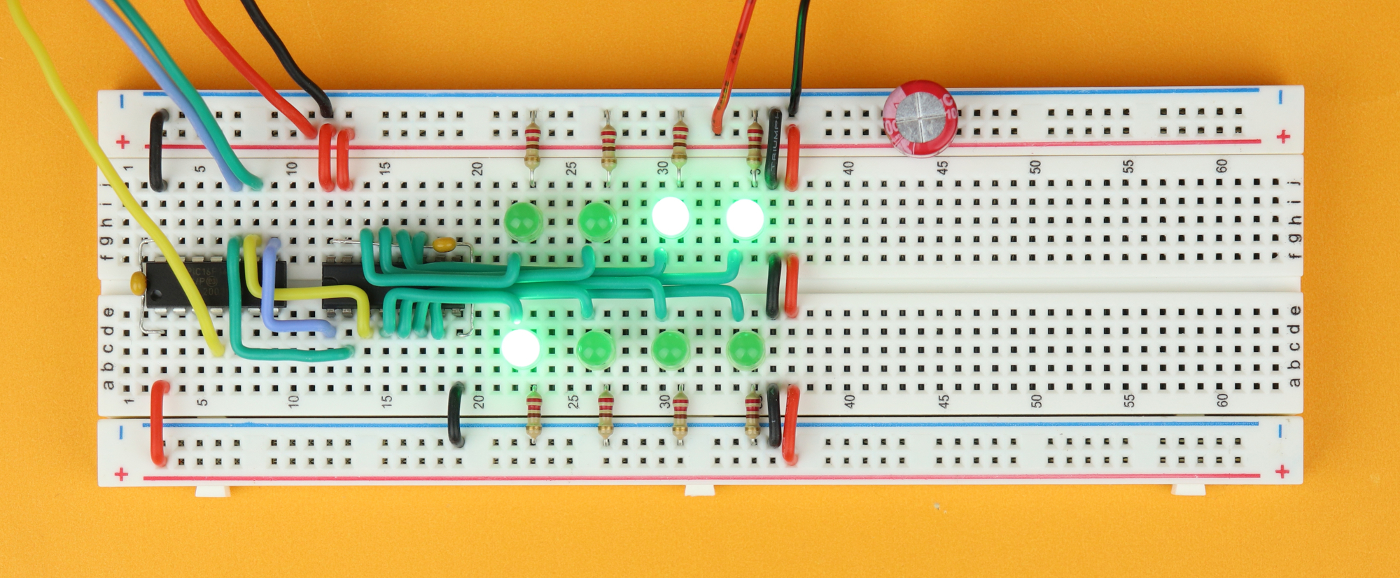
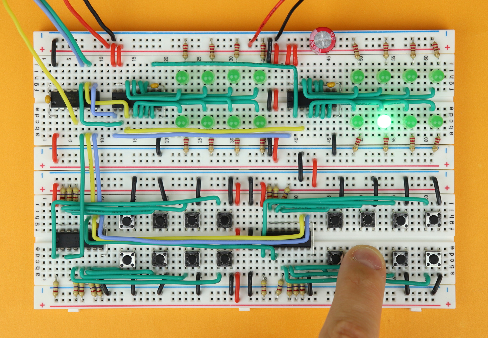
And when we compile the code, we see that the circuit now reacts to us pressing the buttons:
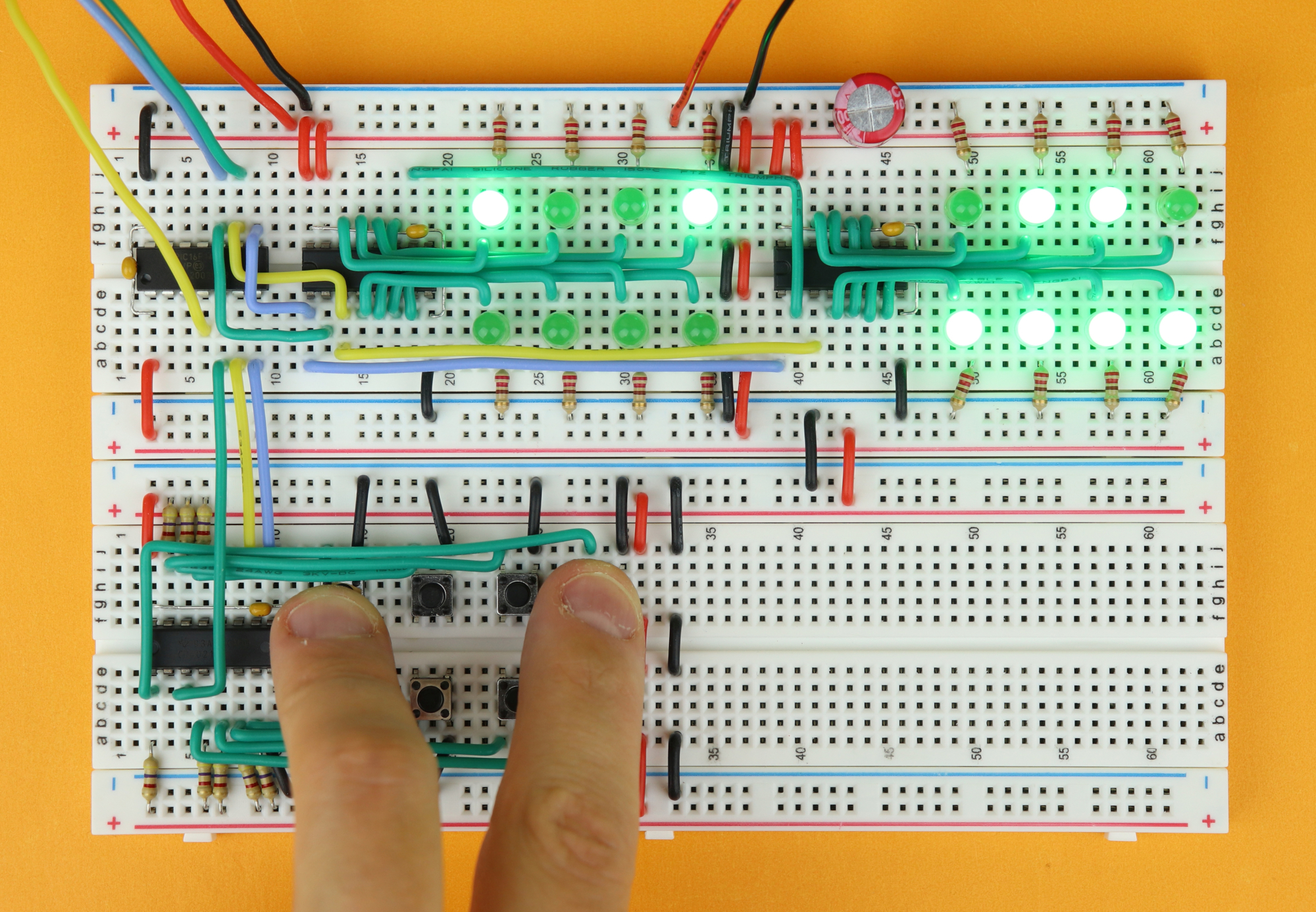
The left set of LEDs shows the inverted signals (~v1, LED on = button pressed) and the right set of LEDs shows the signals as-is (v1, LED on = button not pressed).
Reading out an additional CD4021
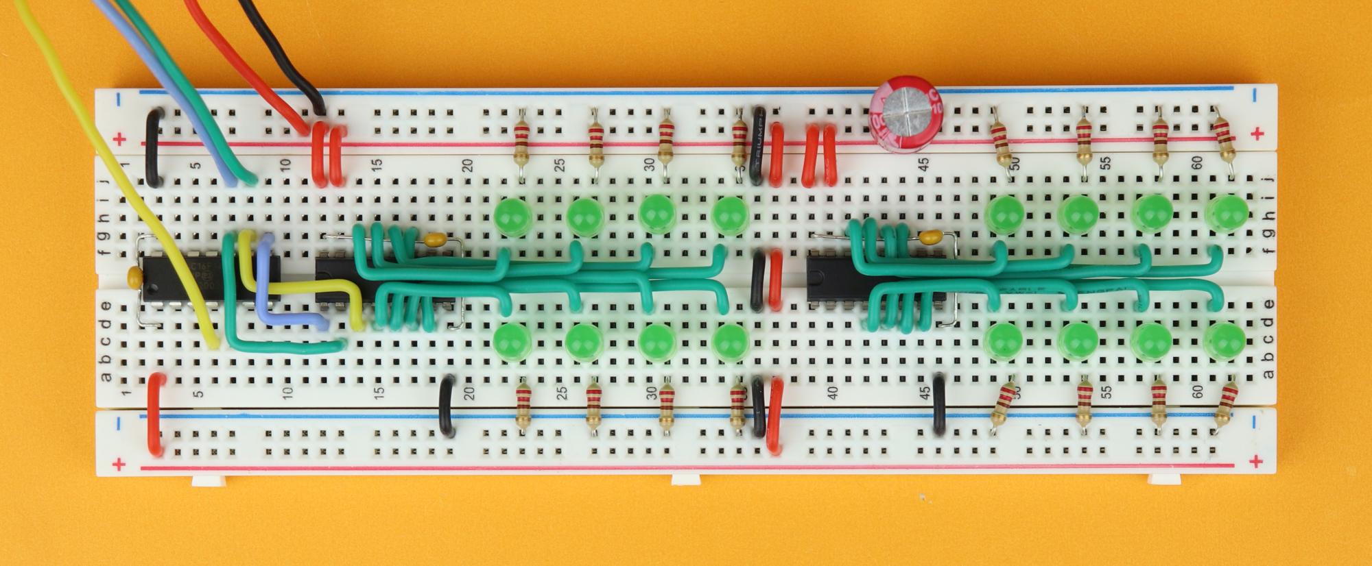
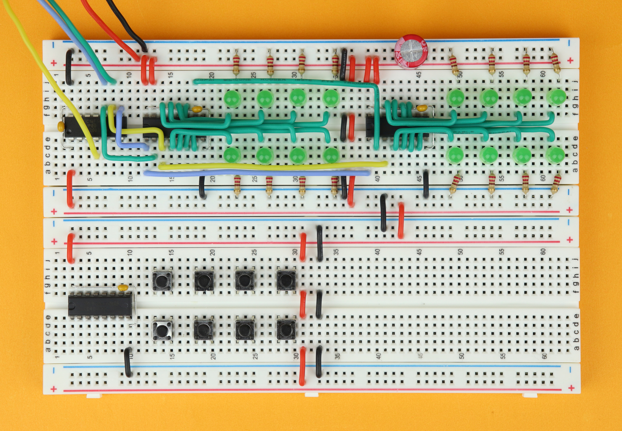
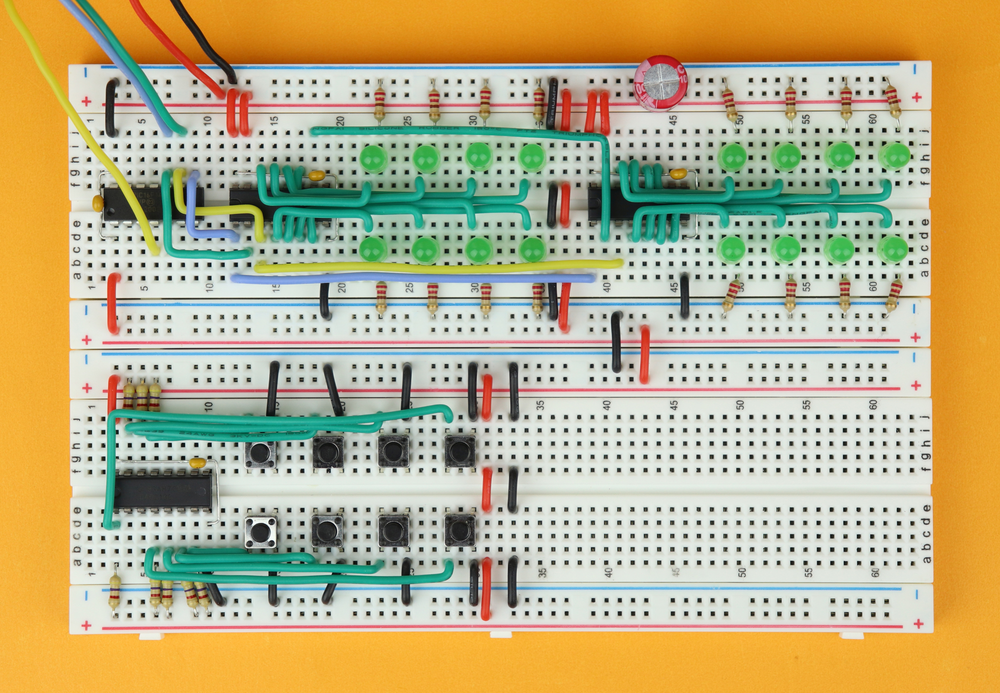
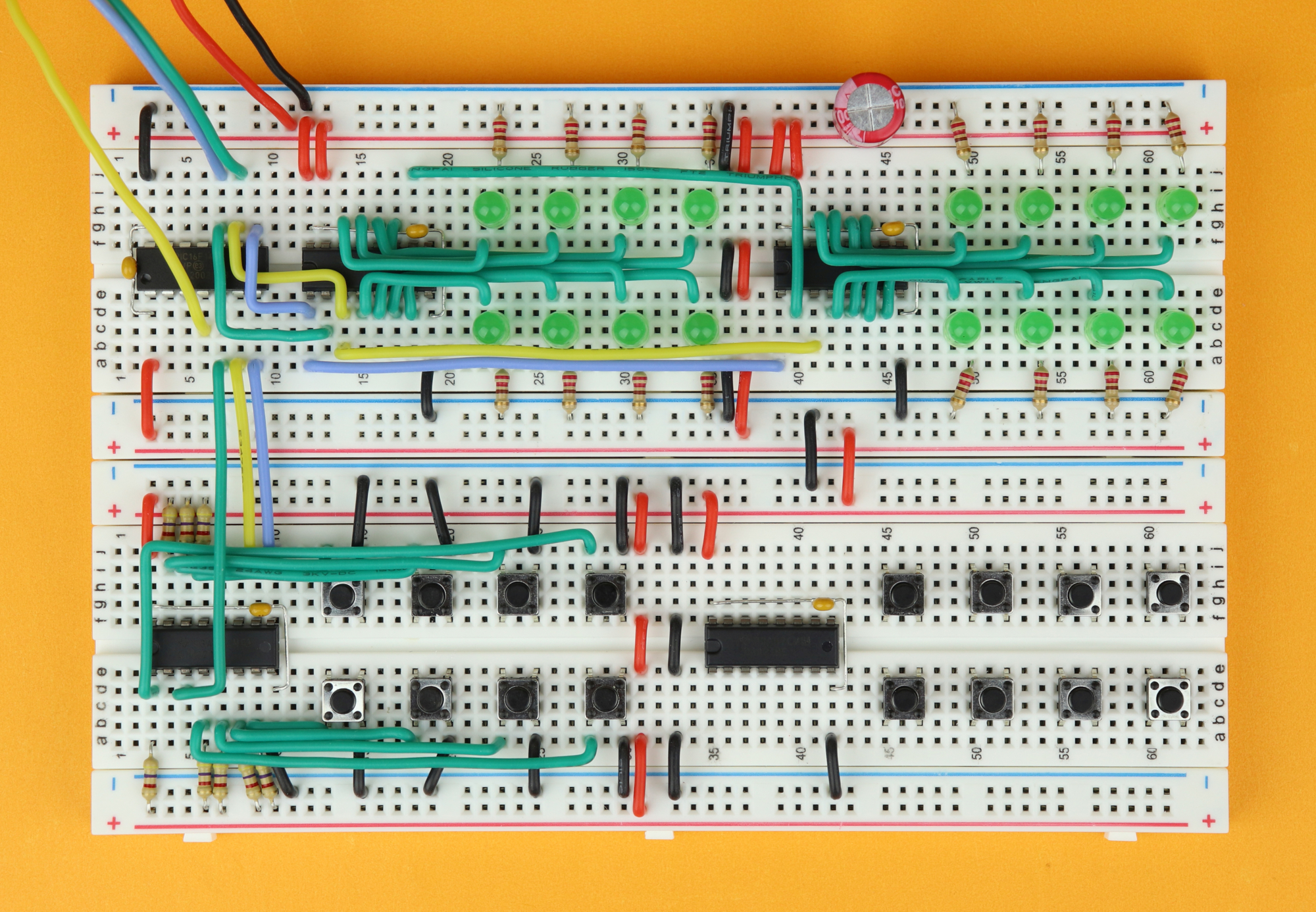
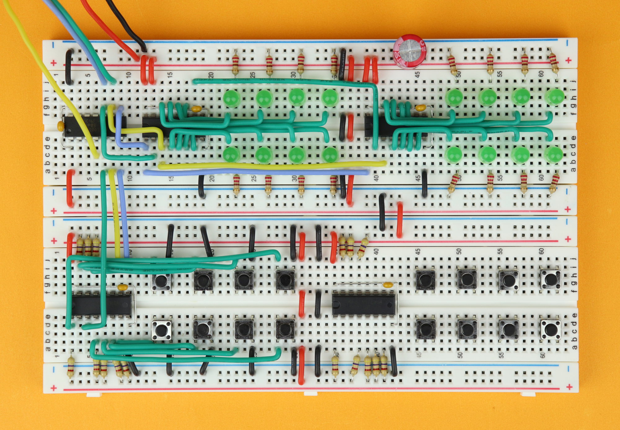
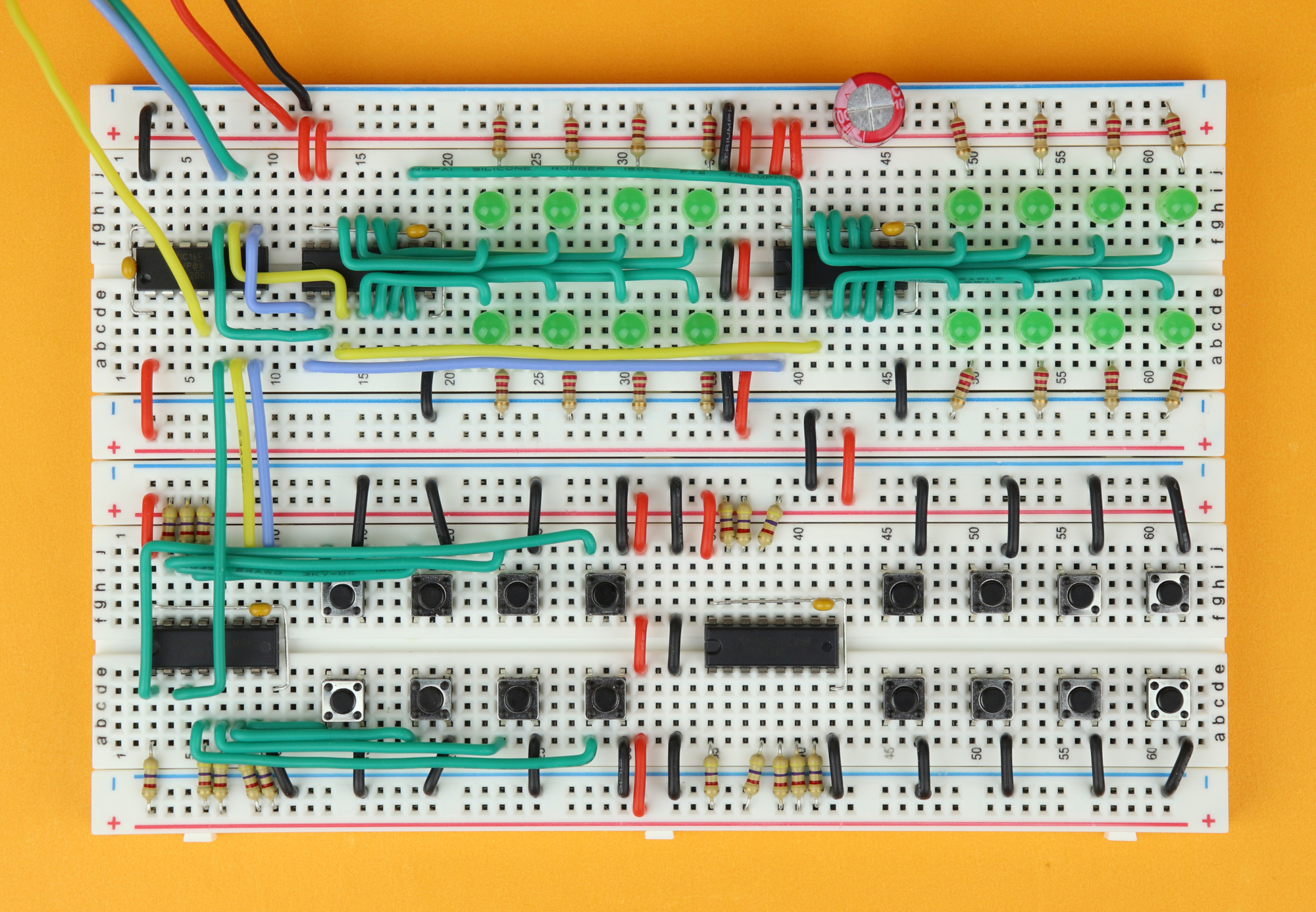
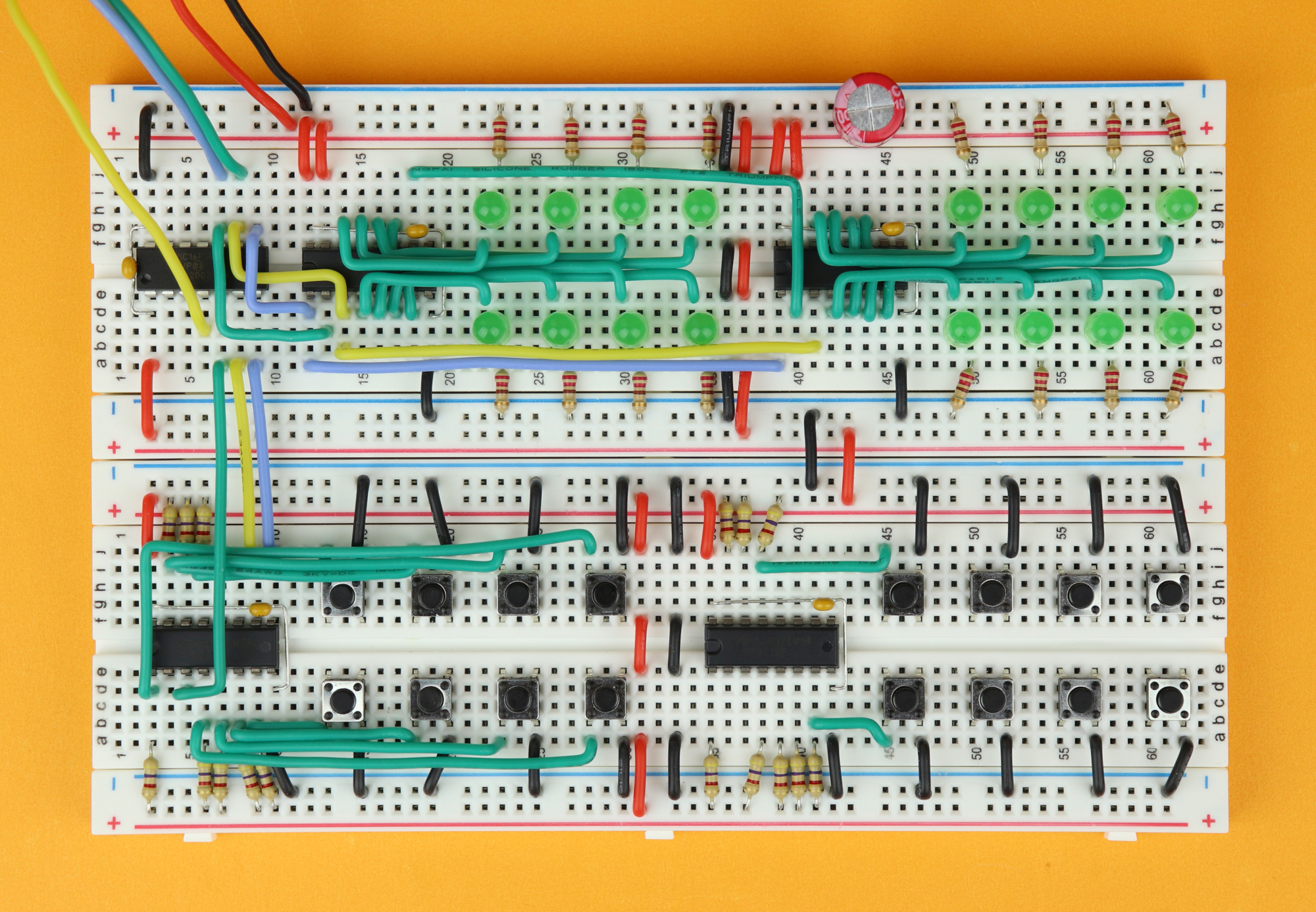
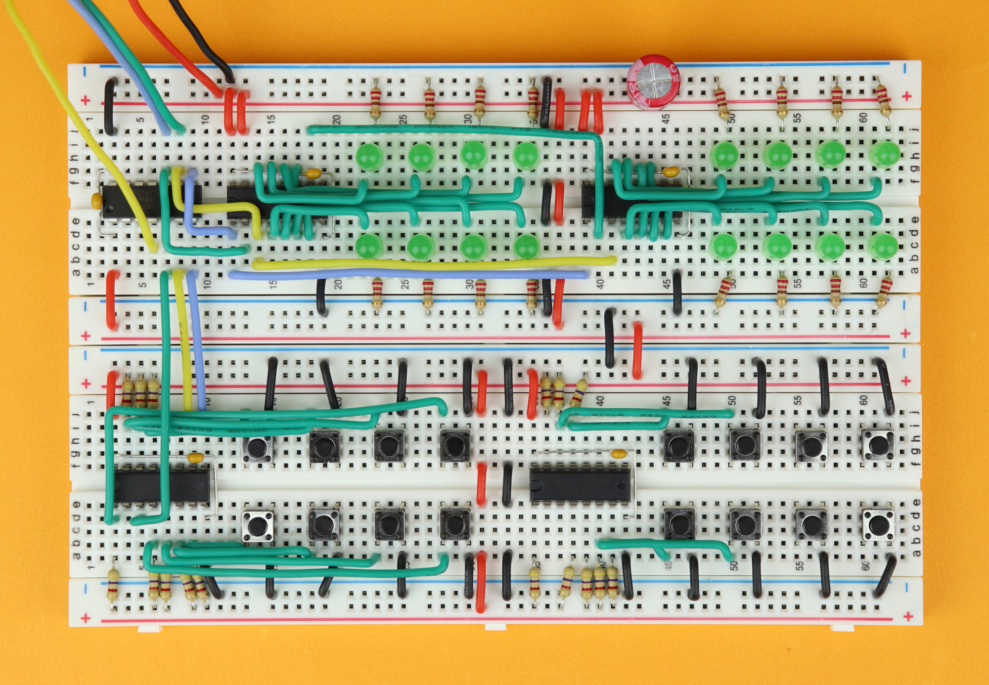
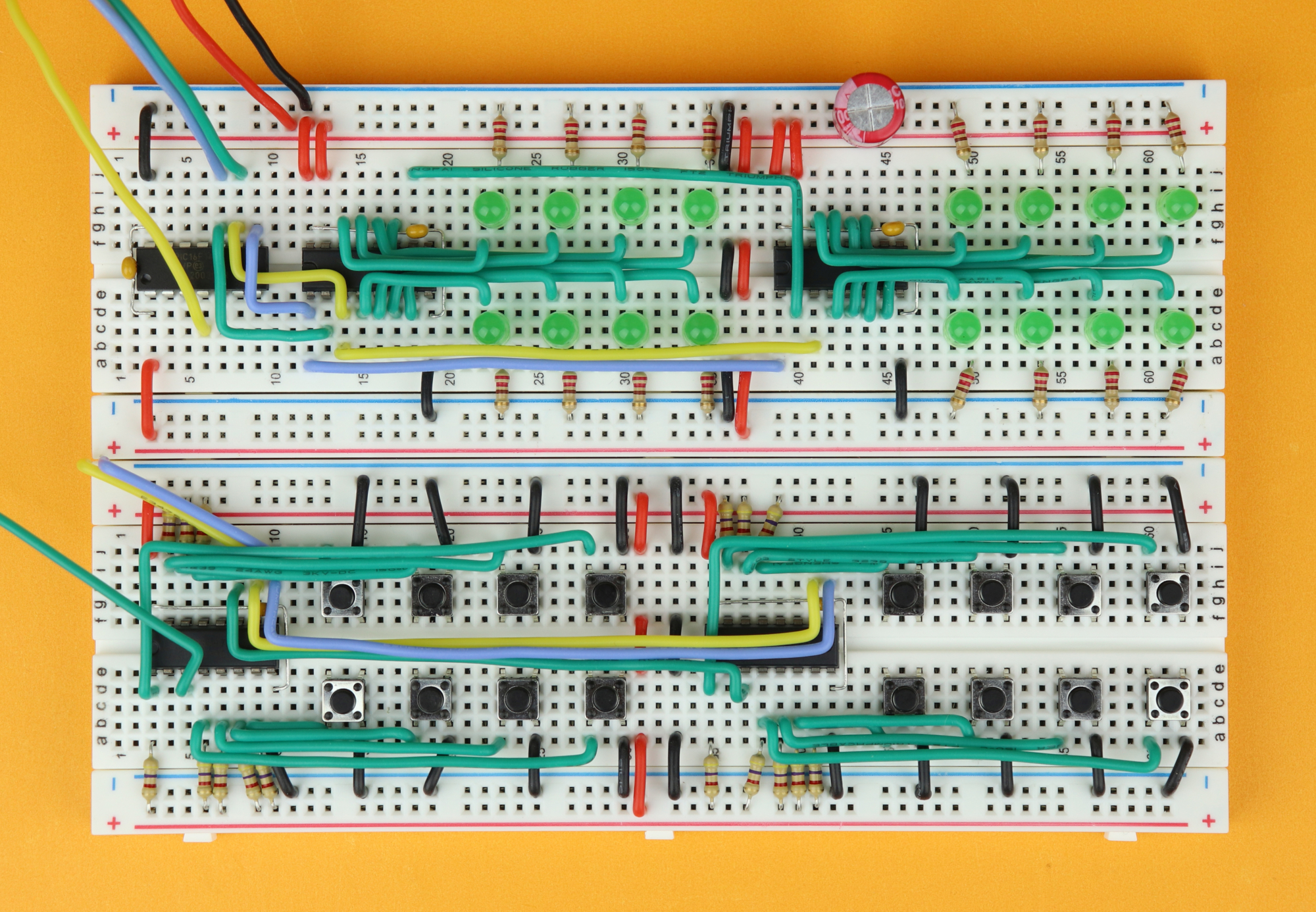
And you saw that one coming from a mile away: let's add another CD4021! Here is how we do that:
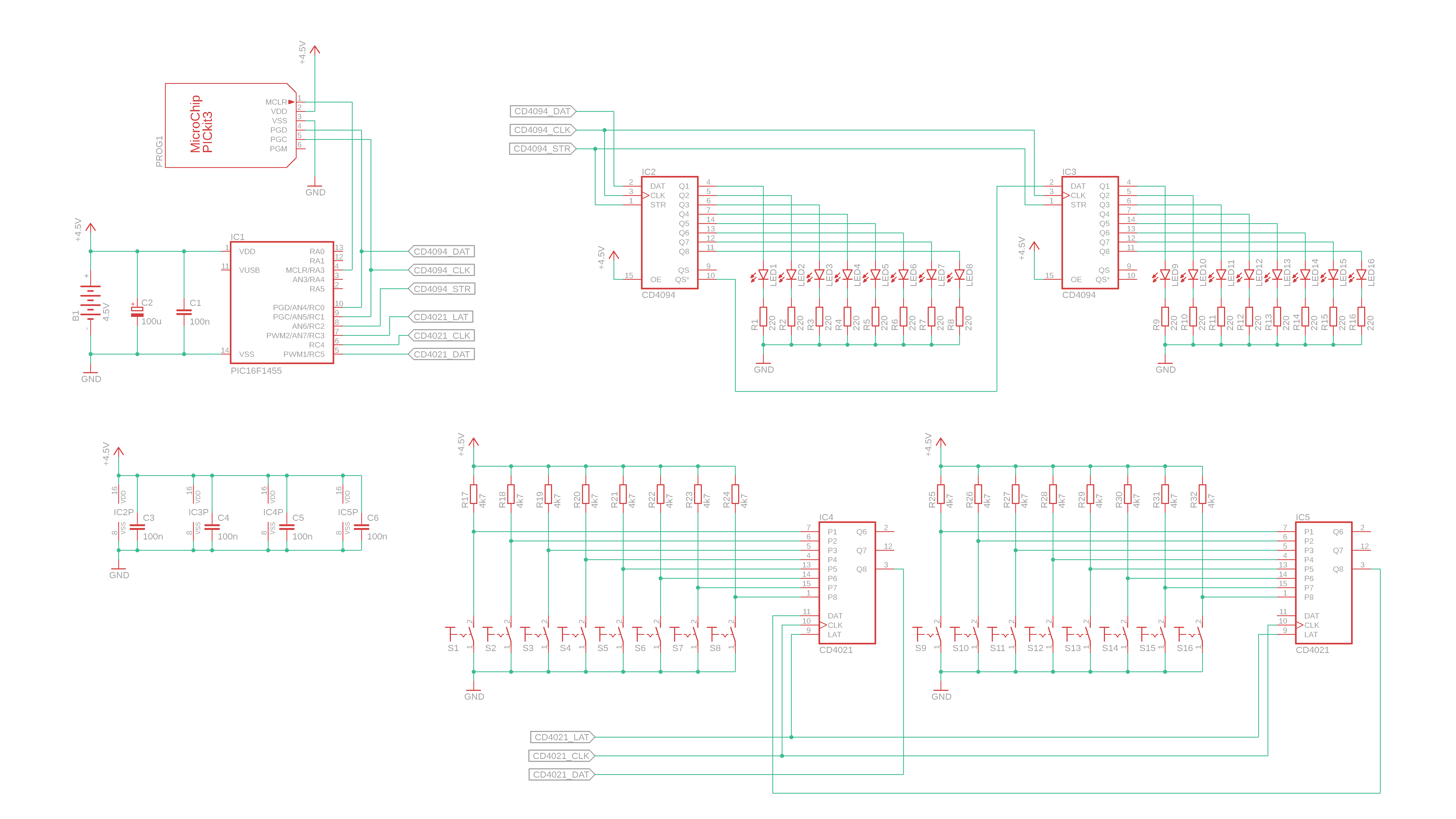
Everything at the CD4021 is connected as before, except for the DATA and Q8 pin: the Q8 output of IC5 is connected to the DATA input of IC4. This way, the data travels out of IC5 into IC4, and then into the PIC16F1455. This is the reason why again we do not need an additional connection to the PIC16F1455, which makes shift registers so powerful.
CLOCK and LATCH are connected in parallel, and everything else is really as before. So now let's build it!
-

-
Step 36
Remove the power.
-
-
Step 37
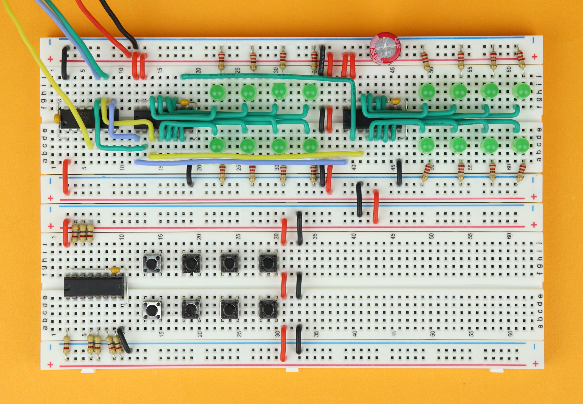
Insert the CD4021 in row 35, with its notch facing to the left. Connect VDD at pin 16, and GROUND at pin 8. Insert the 100nF bypass capacitor C5 between pins 16 and 8, close to the chip.
-
-
Step 38
Insert the eight pushbuttons in rows 45, 50, 55, and 60, on both the upper side and the lower side of the breadboard.
-
-
Step 39
Insert the 4.7kΩ pullup resistors R25–R32 from the P1–P8 inputs of the CD4021 to VDD (pins 1, 4, 5, 6, 7, 13, 14, and 15).
-
-
Step 40
Connect the right terminal of each pushbutton to the ground rail.
-
-
Step 41
Now it's time to connect the other terminal to the CD4021 inputs as well, and it works out nicely if you do it in pairs again.
Connect P1 at pin 7 to row 45 (lower part of breadboard) and P5 at pin 13 to row 45 (upper part of breadboard).
-
-
Step 42
Connect P2 at pin 6 to row 50 (lower part of breadboard) and P6 at pin 14 to row 50 (upper part of breadboard).
-

-
Step 43
Connect P3 at pin 5 to row 55 (lower part of breadboard) and P7 at pin 15 to row 55 (upper part of breadboard).
-
-
Step 44
Connect P4 at pin 4 to row 60 (lower part of breadboard), and, last, P8 at pin 1 (lower part of breadboard) to row 60 on the upper part of the breadboard.
-
-
Step 45
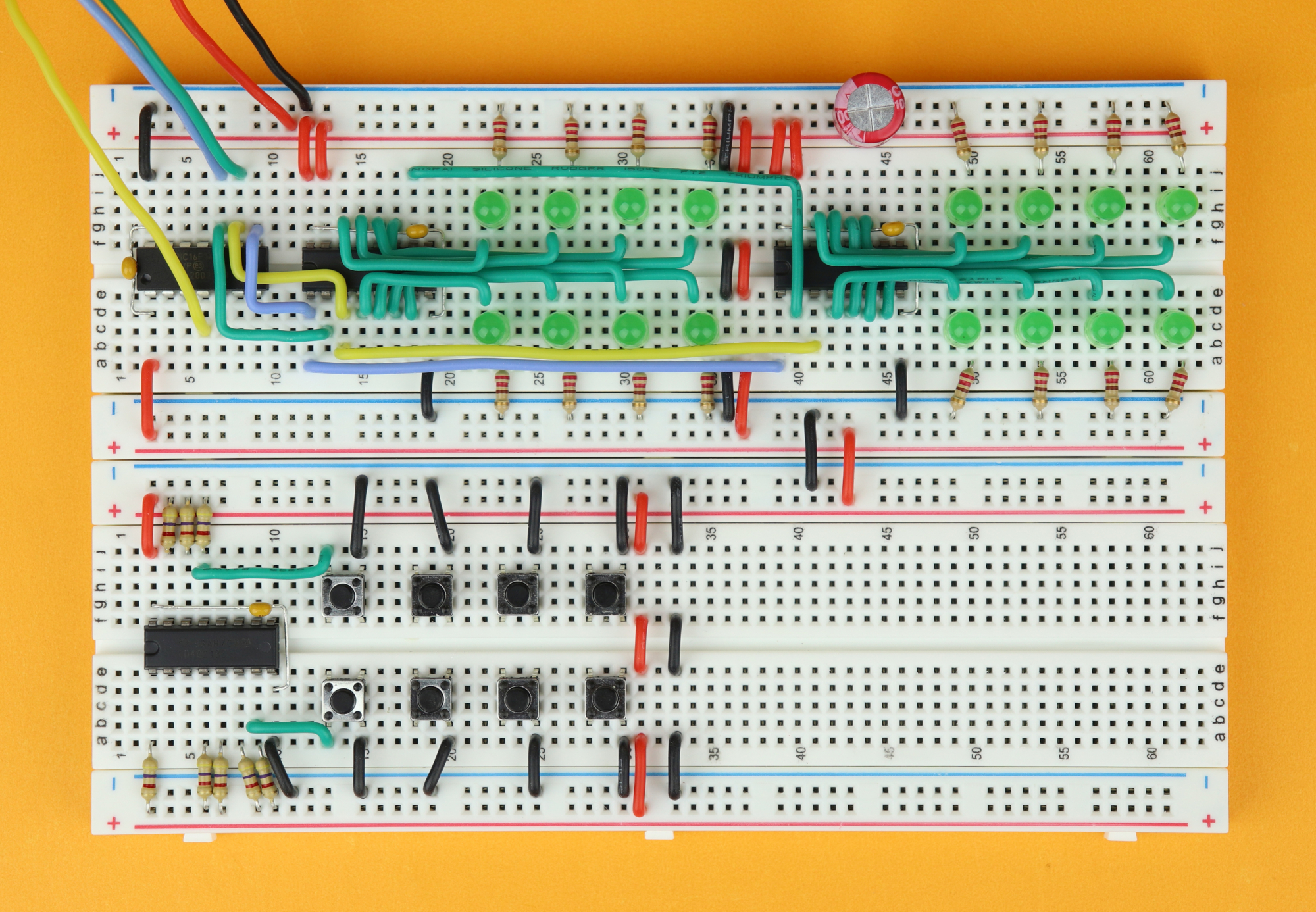
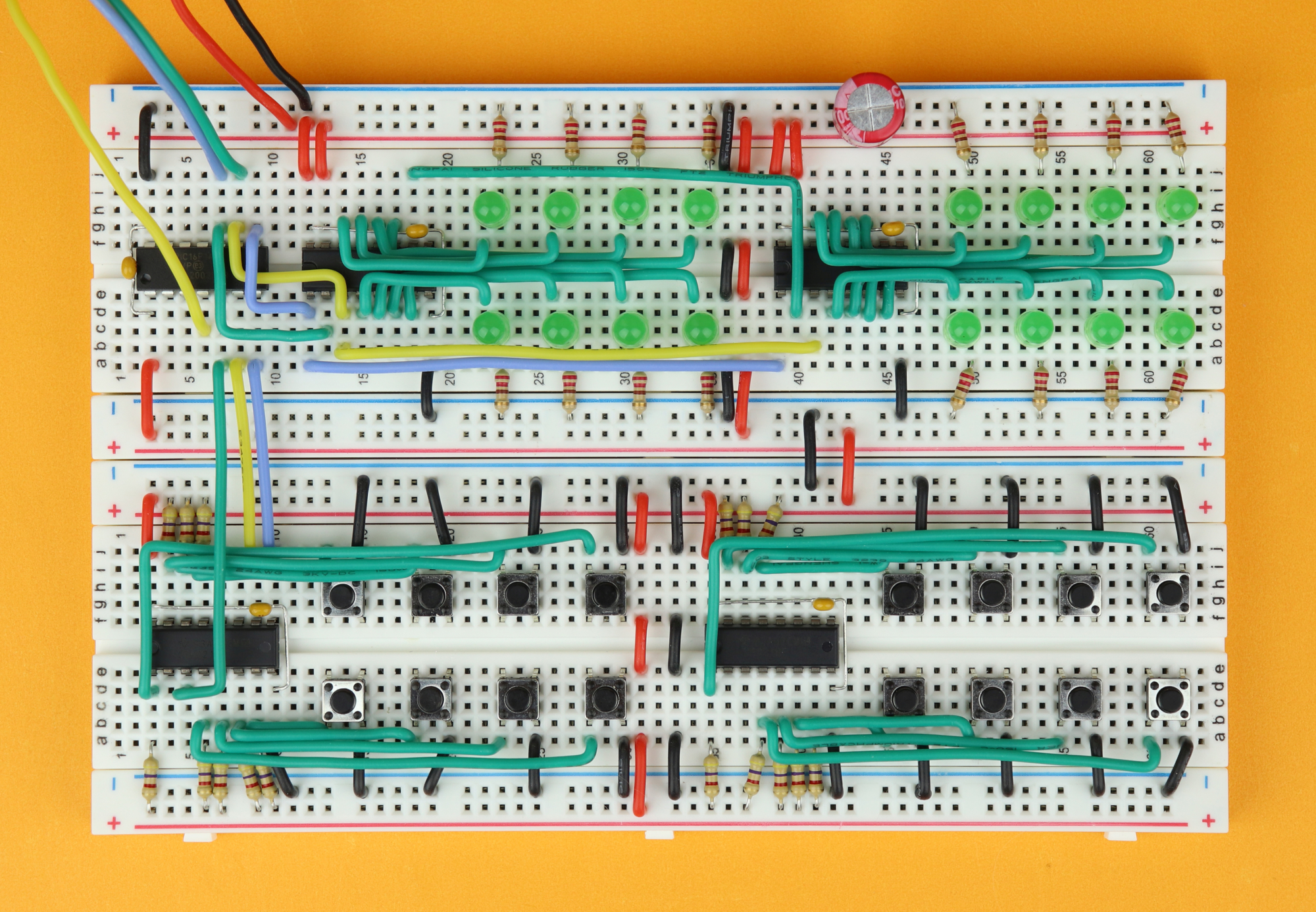
Now it's time to connect the CD4021 to the previous CD4021. CLOCK (yellow wire) goes from pin 10 of this CD4021 to pin 10 of the previous CD4021; LATCH (blue wire) goes from pin 9 of this CD4021 to pin 9 of the previous CD4021. Connect the Q8 output at pin 3 of this CD4021 to the DATA input at pin 11 of the previous CD4021.
-
-
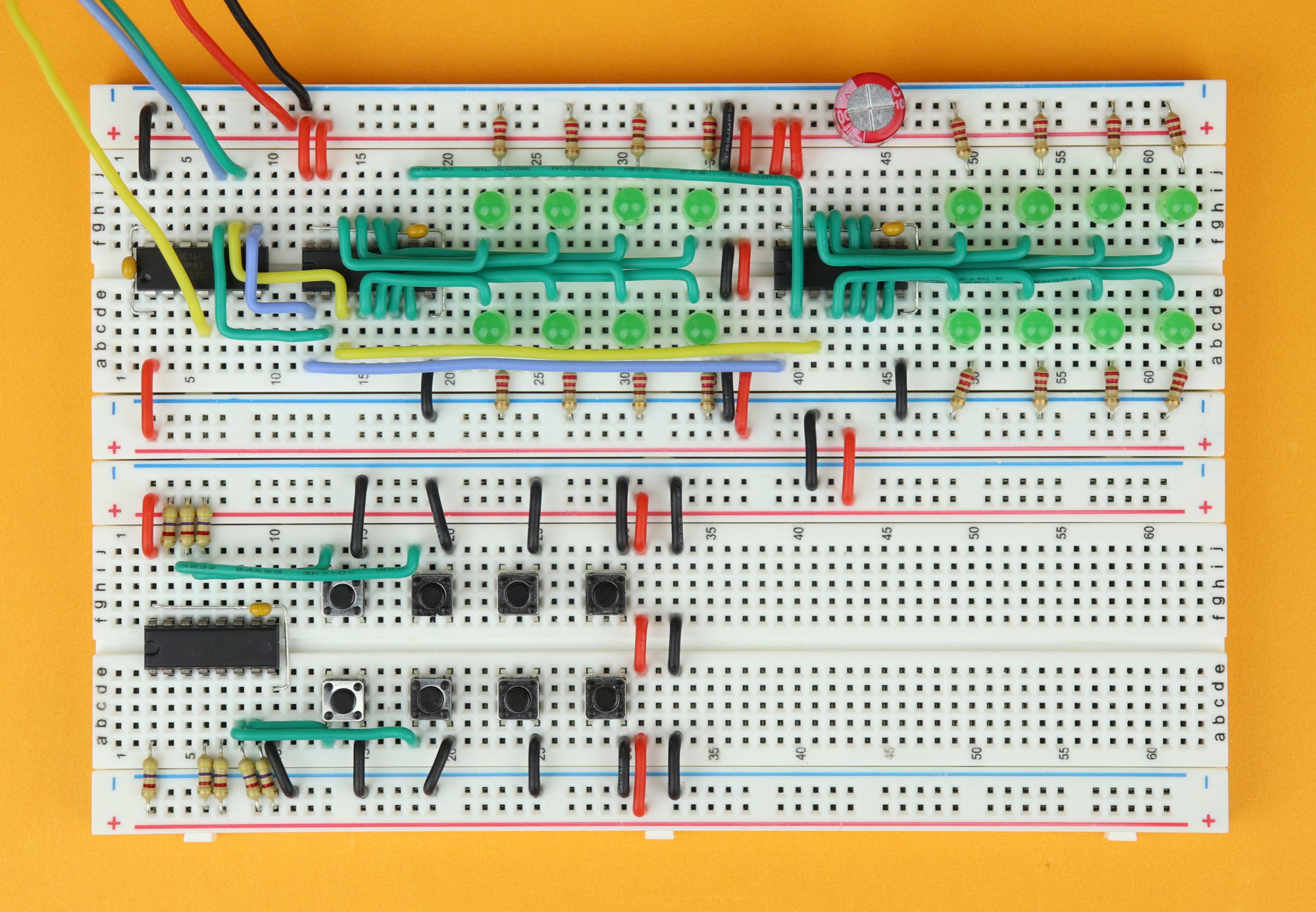
Step 46
And, finally, plug the power back in.
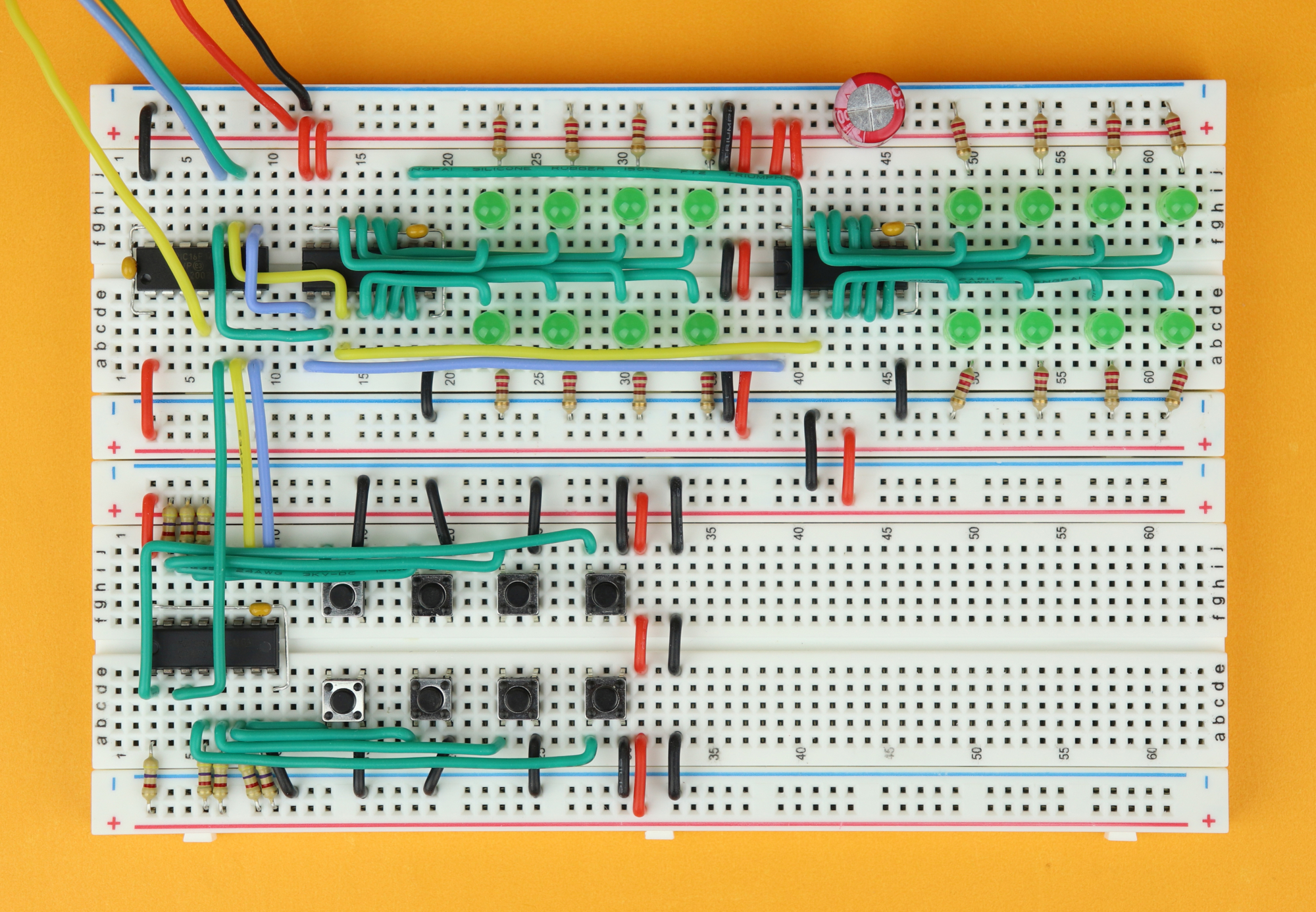
And, you may have guessed, the code is again not so complicated because we just need to add a very few things.
// input values
unsigned char v1 = 0;
unsigned char v2 = 0;- Because we are reading out two sets of eight buttons we need another variable to store the status of the second set of buttons.
// main loop
    while (1) {

        // read out 16 buttons (two bytes)
        CD4021_load();
        v1 = CD4021_read();
        v2 = CD4021_read();

		// send out the information
		// (and invert each bit, because of the pullup resistors)
		CD4094_send(~v2);
        CD4094_send(~v1);
        CD4094_load();

}- And we again just duplicate our previous line into two lines (76 and 77).
- The information in
v1is received first, and that's the data from the closest CD4021 shift register in the chain (IC4; the buttons on the left). The variablev2contains the buttons from the shift register one step further in the chain (IC5; the buttons on the right). - Then we send out
~v2and~v1, so that the LEDs show the status of our buttons. We send out~v2first, so that it shows up on the right set of LEDs, and~v1second, so that it appears on the left set of LEDs. - Sounds confusing, I know. It helps to just program this, and play around with it in real life :) Give it a go!
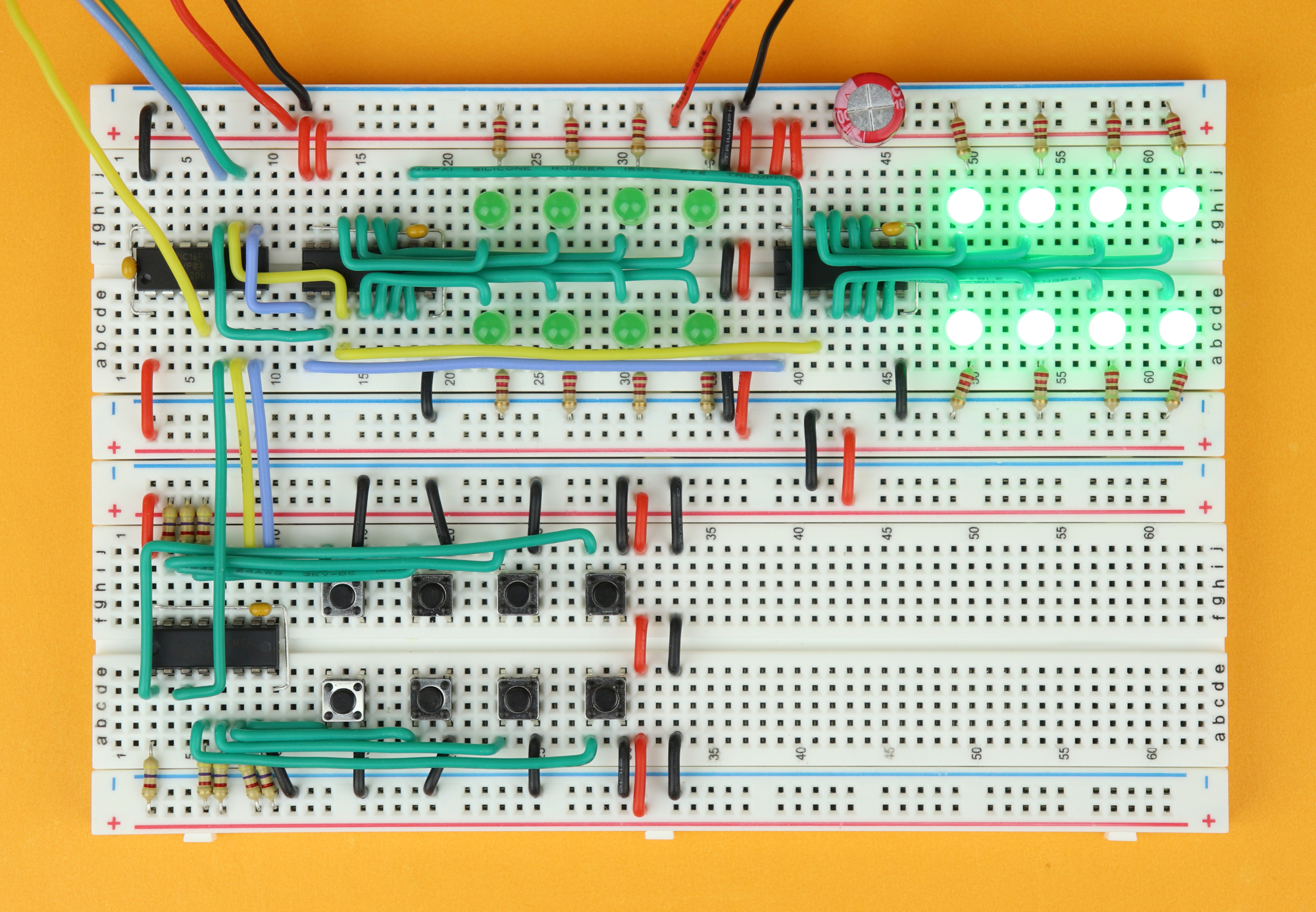
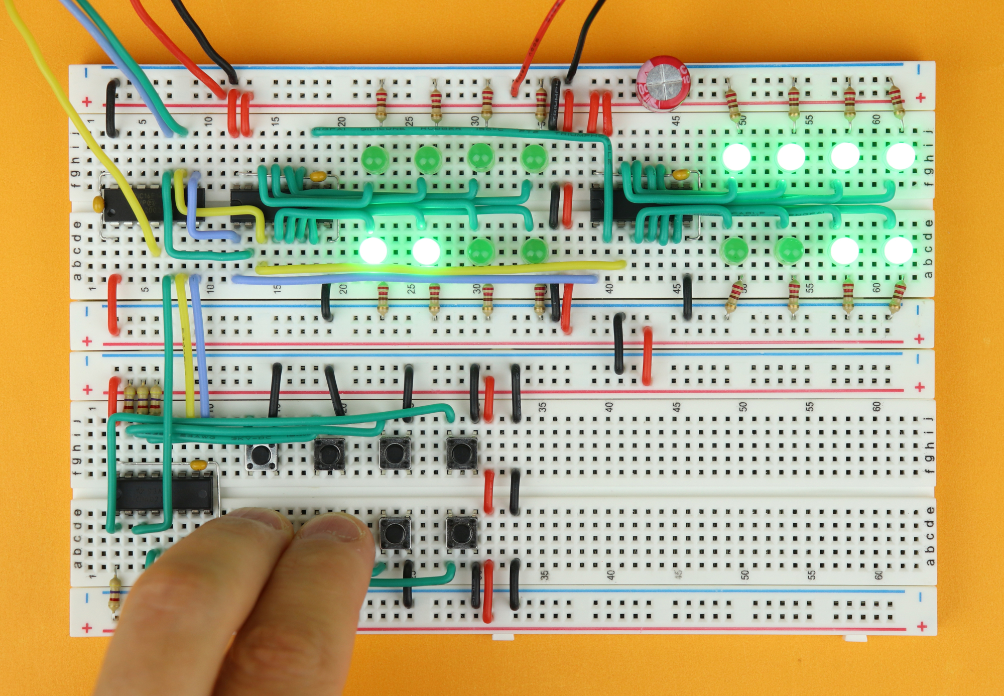
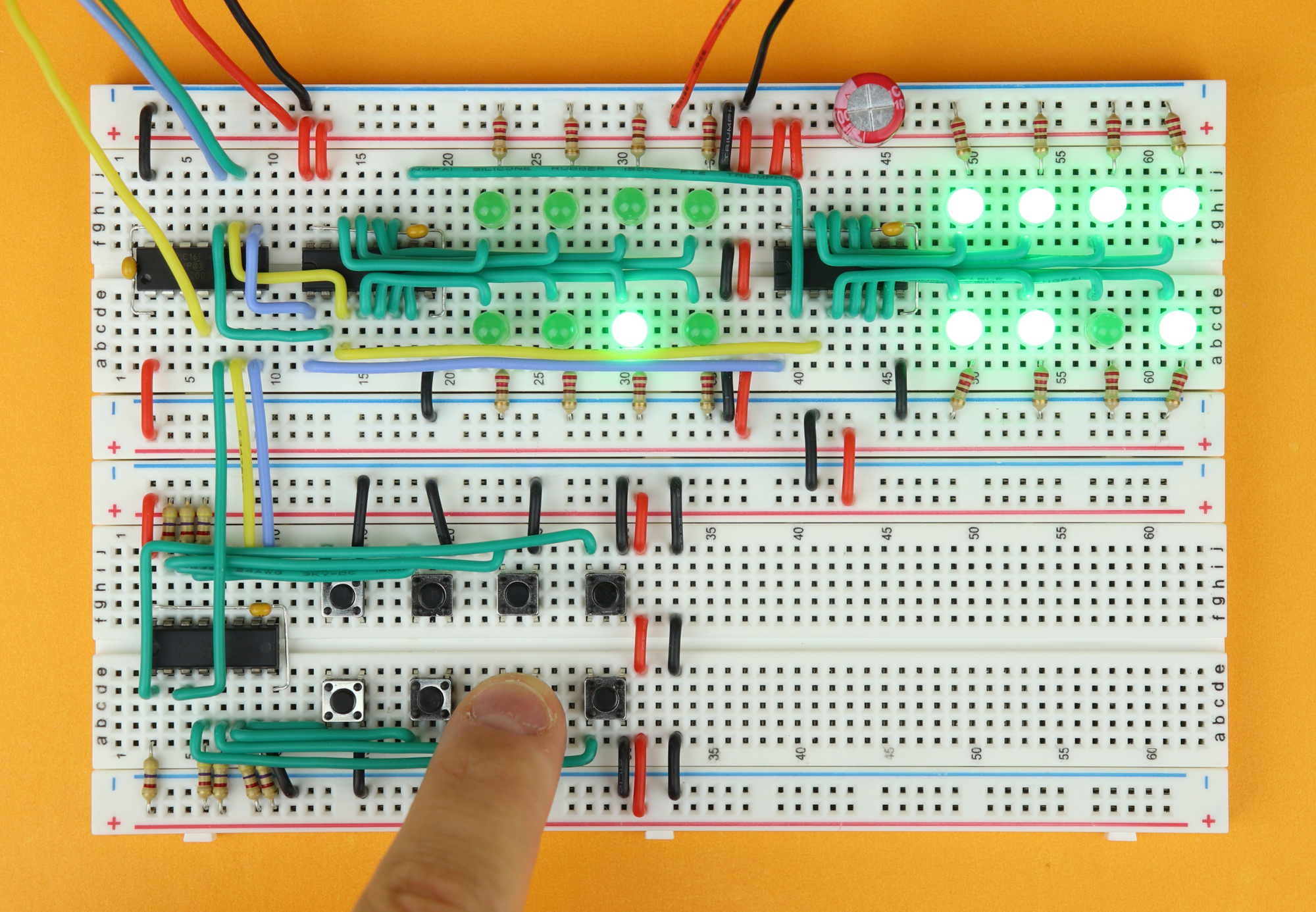
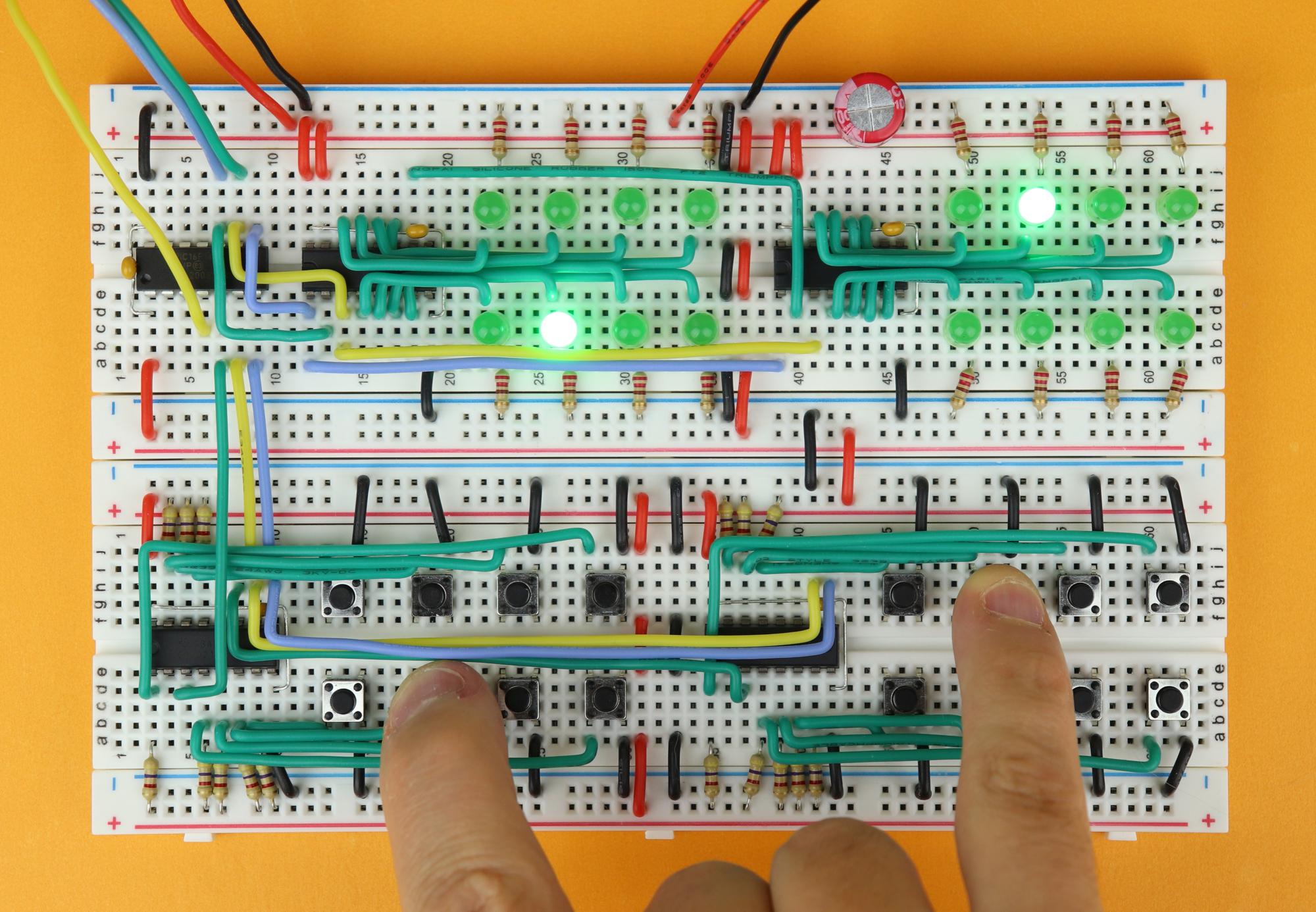
And, sure enough, after flashing the LEDs react to our button presses:
Reading out a game controller
Okay, let's put it to a test!
The funny thing is that the lower part with the CD4021's is almost exactly what is included in a vintage SNES game controller. "Almost exactly" because these controllers have 12 buttons in total, and not sixteen, but everything else is exactly the same.
This is one of those newly made SNES controllers:

And here is the pinout:
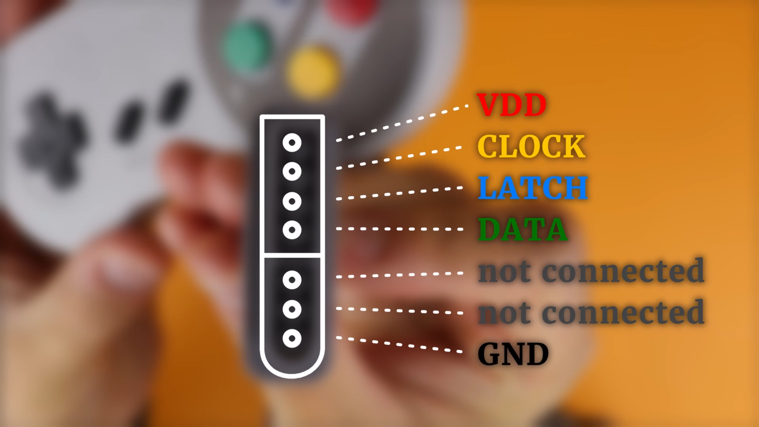
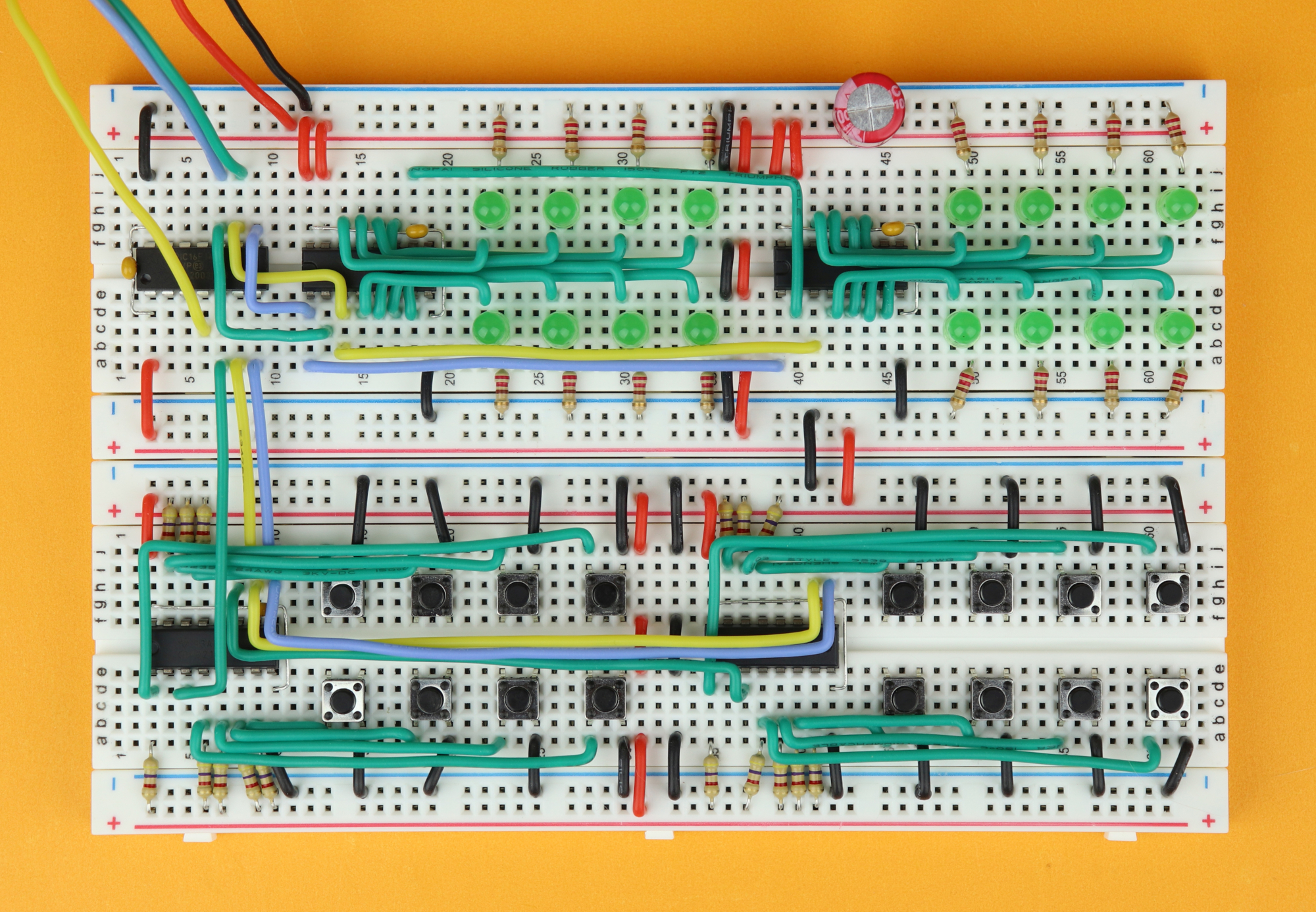
So you see: these are exactly the connections we need for our CD4021 setup (NC means "not connected" so we can just ignore those two wires)! It is a bit hard to find adapters for the SNES, so I just bought an adapter cable, cut it in half, and soldered wires to one end to plug it into the breadboard. I used a continuity meter to figure out which wire goes to which pin of the plug, and here is the final result:
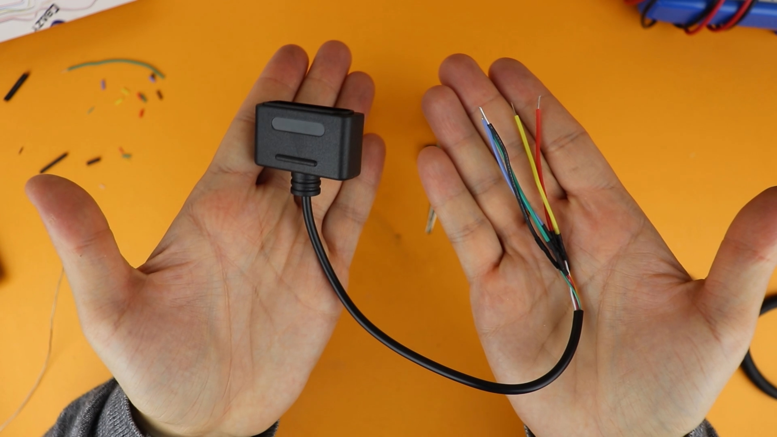
And just so that I don't confuse myself I used the same colors we used before (red=VDD, black=GROUND, green=DATA, yellow=CLOCK, and blue=LATCH). Let's connect it all up!
-

-
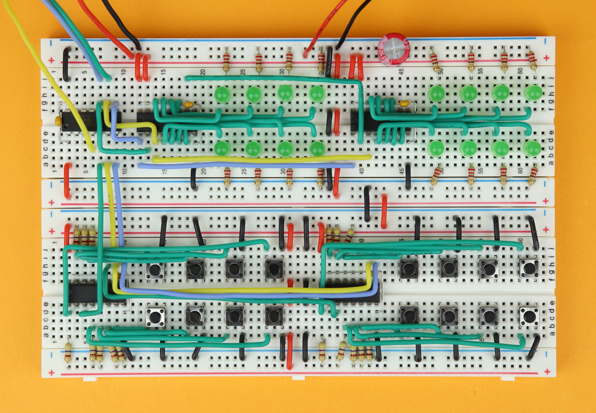
Step 47
First, remove the DATA, CLOCK, and LATCH wires at pins 5, 6, and 7 of the PIC16F1455.
-
-
Step 48
Remove the VDD and GROUND connection between the two breadboards.
-
-
Step 49
Now you can remove the lower breadboard entirely.
-

-
Step 50
Insert the SNES adapter cable. Red (VDD) and black (GROUND) can be connected to the power rail; DATA (green) goes into pin 5 of the PIC16F1455, CLOCK (yellow) goes into pin 6, and LATCH (blue) goes into pin 7 of the PIC16F1455. And that's it! Plug the power back in, and it's working!
Yup, no coding needed anymore, this is what happens when you press the buttons:
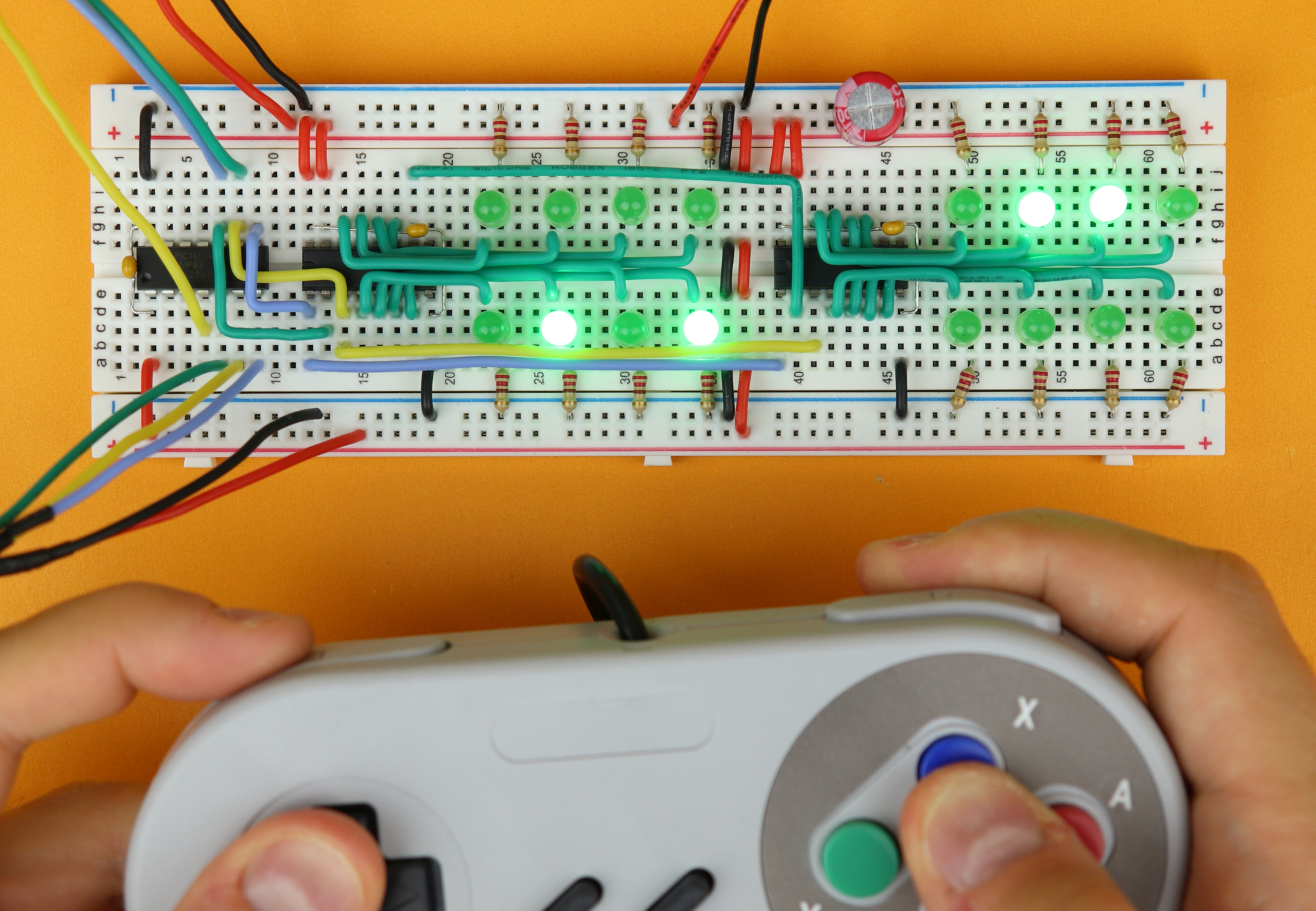
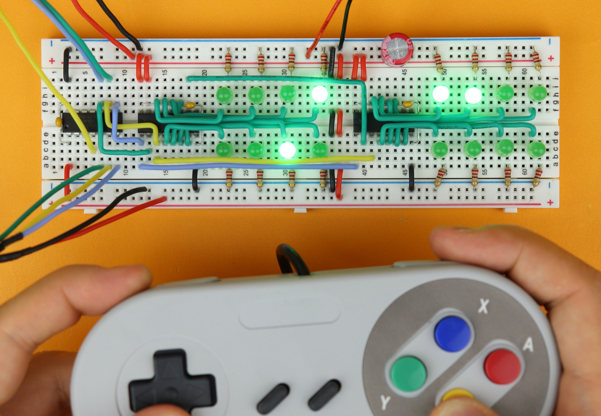
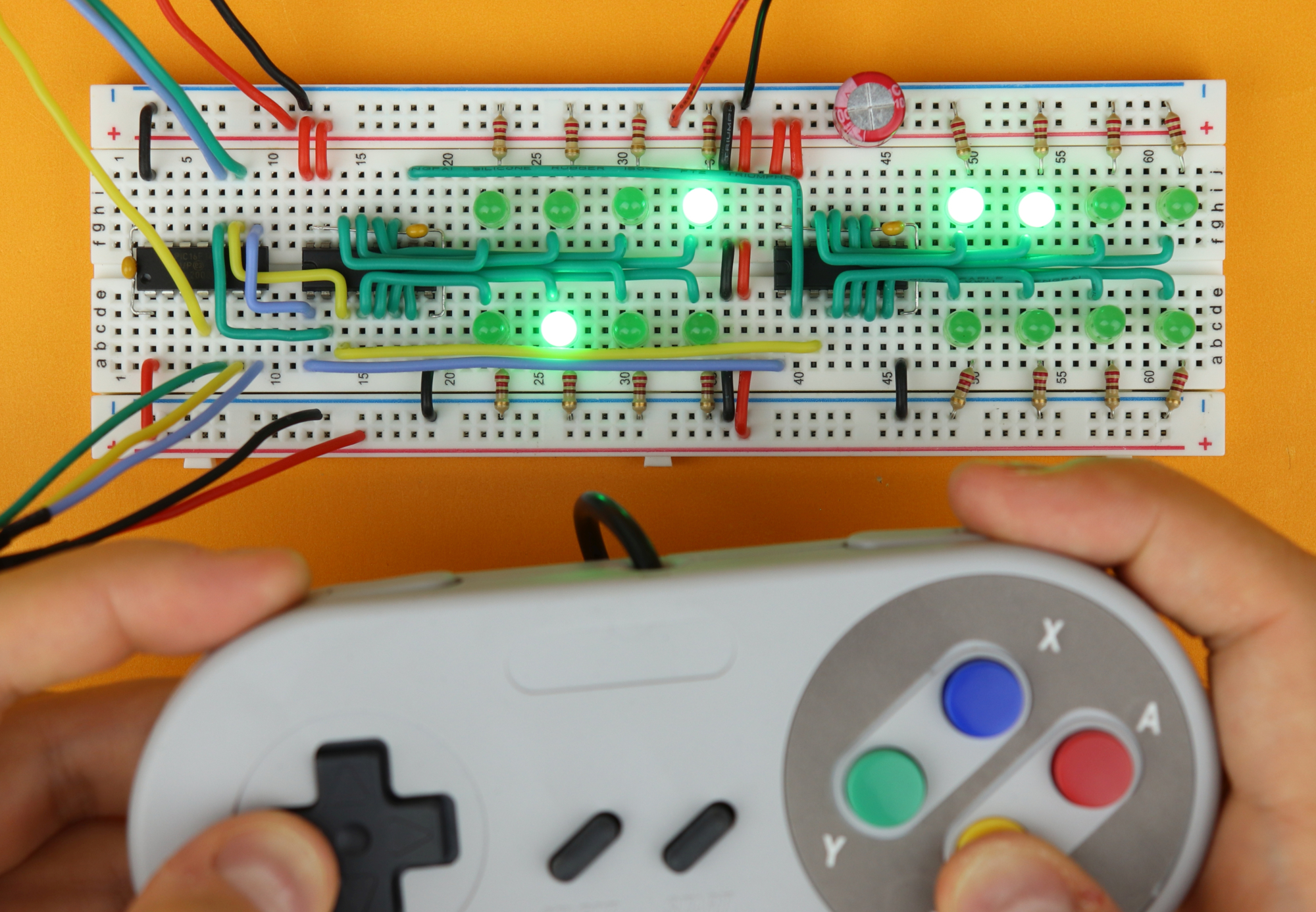
Now of course it is nice to be able to react to some button presses, and for that we actually do need to add some code. But we can use our existing code to make our life simpler. For example, this here is what happens when you press button A:

This is LED Q8 of the second shift register, which means the eighth bit in v2 encodes that button. So here is the code of how we react to all of these buttons:
		// react specifically to SNES buttons

		// up
		if ((~v1) & 0b00001000) {

		}
		// down
		if ((~v1) & 0b00000100) {

		}
		// left
		if ((~v1) & 0b00000010) {

		}
		// right
		if ((~v1) & 0b00000001) {

		}
		// left shoulder
		if ((~v2) & 0b00100000) {

		}
		// right shoulder
		if ((~v2) & 0b00010000) {

		}
		// A
		if ((~v2) & 0b10000000) {

		}
		// B
		if ((~v1) & 0b10000000) {

		}
		// X
		if ((~v2) & 0b01000000) {

		}
		// Y
		if ((~v1) & 0b01000000) {

		}
		// select
		if ((~v1) & 0b00100000) {

		}
		// start
		if ((~v1) & 0b00010000) {

		}
Of course all of these if-statements are still empty, but now it's your turn: put in the code that you want, and use such a controller in one of your next projects :)
YouTube video
I covered this entire tutorial in a dedicated YouTube video:
Final thoughts

I had a lot of fun with this tutorial, and I hope that it will be useful for you and inspires you to use shift registers in one of your future project. They are incredibly versatile and you can use them in many many different cases.
And if the whole coding microcontroller stuff was a bit much for you, don't worry. Why don't you check out my PIC introduction article (it also has a video!), after which you can easily follow all of the microcontroller tutorials and projects here on this channel.
Thank you so much for watching, let me know what else you want to learn, and I will see you next time!
Appendix: full source code
Here you can find the full dot matrix source code. The code (as well as the .hex file) are also available for download in the resources box.
/*
 * File:   main.c
 * Author: boos
 *
 * Created on October 17, 2022, 6:11 PM
 */

// CONFIG1
#pragma config FOSC = INTOSC    // Oscillator Selection Bits (INTOSC oscillator: I/O function on CLKIN pin)
#pragma config WDTE = OFF       // Watchdog Timer Enable (WDT disabled)
#pragma config PWRTE = OFF      // Power-up Timer Enable (PWRT disabled)
#pragma config MCLRE = OFF      // MCLR Pin Function Select (MCLR/VPP pin function is digital input)
#pragma config CP = OFF         // Flash Program Memory Code Protection (Program memory code protection is disabled)
#pragma config BOREN = OFF      // Brown-out Reset Enable (Brown-out Reset disabled)
#pragma config CLKOUTEN = OFF   // Clock Out Enable (CLKOUT function is disabled. I/O or oscillator function on the CLKOUT pin)
#pragma config IESO = OFF       // Internal/External Switchover Mode (Internal/External Switchover Mode is disabled)
#pragma config FCMEN = OFF      // Fail-Safe Clock Monitor Enable (Fail-Safe Clock Monitor is disabled)

// CONFIG2
#pragma config WRT = OFF        // Flash Memory Self-Write Protection (Write protection off)
#pragma config CPUDIV = CLKDIV6 // CPU System Clock Selection Bit (CPU system clock divided by 6)
#pragma config USBLSCLK = 48MHz // USB Low SPeed Clock Selection bit (System clock expects 48 MHz, FS/LS USB CLKENs divide-by is set to 8.)
#pragma config PLLMULT = 3x     // PLL Multipler Selection Bit (3x Output Frequency Selected)
#pragma config PLLEN = ENABLED  // PLL Enable Bit (3x or 4x PLL Enabled)
#pragma config STVREN = ON      // Stack Overflow/Underflow Reset Enable (Stack Overflow or Underflow will cause a Reset)
#pragma config BORV = LO        // Brown-out Reset Voltage Selection (Brown-out Reset Voltage (Vbor), low trip point selected.)
#pragma config LPBOR = OFF      // Low-Power Brown Out Reset (Low-Power BOR is disabled)
#pragma config LVP = OFF        // Low-Voltage Programming Enable (High-voltage on MCLR/VPP must be used for programming)

#include <xc.h>

// define functions
void CD4094_send (unsigned char d);
void CD4094_load (void);
unsigned char CD4021_read (void);
void CD4021_load (void);

// input values
unsigned char v1 = 0;
unsigned char v2 = 0;

// abbreviations for convenience
#define CD4094_DAT RC0
#define CD4094_CLK RC1
#define CD4094_STR RC2
#define CD4021_DAT RC5
#define CD4021_CLK RC4
#define CD4021_LAT RC3

// main function
void main (void) {


    // set up ports RC0:4 as outputs
    TRISC0 = 0;
    TRISC1 = 0;
    TRISC2 = 0;
    TRISC3 = 0;
    TRISC4 = 0;

    // set up port RC5 as input
    TRISC5 = 1;

	// disable analog features on ports RC0, RC1, RC2, and RC3
    ANSC0 = 0;
    ANSC1 = 0;
    ANSC2 = 0;
    ANSC3 = 0;


    // main loop
    while (1) {

        // read out 16 buttons (two bytes)
        CD4021_load();
        v1 = CD4021_read();
        v2 = CD4021_read();

		// send out the information
		// (and invert each bit, because of the pullup resistors)
		CD4094_send(~v2);
        CD4094_send(~v1);
        CD4094_load();

		// react specifically to SNES buttons

		// up
		if ((~v1) & 0b00001000) {

		}
		// down
		if ((~v1) & 0b00000100) {

		}
		// left
		if ((~v1) & 0b00000010) {

		}
		// right
		if ((~v1) & 0b00000001) {

		}
		// left shoulder
		if ((~v2) & 0b00100000) {

		}
		// right shoulder
		if ((~v2) & 0b00010000) {

		}
		// A
		if ((~v2) & 0b10000000) {

		}
		// B
		if ((~v1) & 0b10000000) {

		}
		// X
		if ((~v2) & 0b01000000) {

		}
		// Y
		if ((~v1) & 0b01000000) {

		}
		// select
		if ((~v1) & 0b00100000) {

		}
		// start
		if ((~v1) & 0b00010000) {

		}


    }

    return;

}

// This function sends a byte "b" to the CD4094
void CD4094_send (unsigned char b) {

    // send out all eight bits
    for (int i=7; i>=0; i--) {
        CD4094_DAT = (b >> i) & 1;
        CD4094_CLK = 1;
        CD4094_CLK = 0;
    }

}

// This function refreshes the status of all CD4094 outputs
void CD4094_load (void) {

    // refresh the status of all CD4094 outputs
    CD4094_STR = 1;
    CD4094_STR = 0;

}

// This function reads out a byte "b" from the CD4021
unsigned char CD4021_read (void) {

    // initialize the future return value to 0
    unsigned char b = 0;

    // read out all eight bits
    for (int i=7; i>=0; i--) {
        b |= (CD4021_DAT << i);
        CD4021_CLK = 1;
        CD4021_CLK = 0;
    }

    // return the byte
    return b;

}

// This function loads the status of all CD4021 inputs
void CD4021_load (void) {

    // read the status of all CD4021 inputs
    CD4021_LAT = 1;
    CD4021_LAT = 0;

}